The following content is an automatically extracted verbatim text
from the original manufacturer datasheet and is provided for reference purposes only.
View original datasheet text
DDR SDRAM 256Mb F-die (x8, x16)
DDR SDRAM
256Mb F-die DDR400 SDRAM Specification Revision 1.1
Rev. 1.1 August. 2003
DDR SDRAM 256Mb F-die (x8, x16)
256Mb F-die Revision History
Revison 1.0 (June. 2003) 1. First release Revison 1.1 (August. 2003) 1. Added x8 org (K4H560838F)
DDR SDRAM
Rev. 1.1 August. 2003
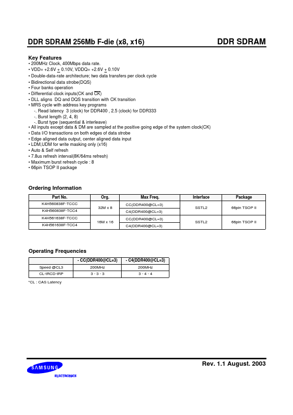
DDR SDRAM 256Mb F-die (x8, x16)
Key Features
• 200MHz Clock, 400Mbps data rate. • VDD= +2.6V + 0.10V, VDDQ= +2.6V + 0.10V • Double-data-rate architecture; two data transfers per clock cycle • Bidirectional data strobe(DQS) • Four banks operation • Differential clock inputs(CK and CK) • DLL aligns DQ and DQS transition with CK transition • MRS cycle with address key programs -. Read latency 3 (clock) for DDR400 , 2.5 (clock) for DDR333 -. Burst length (2, 4, 8) -.
 K4H560838F-TCC4 Datasheet