Description
SYMBOL
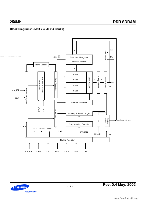
CK, CK
DDR SDRAM
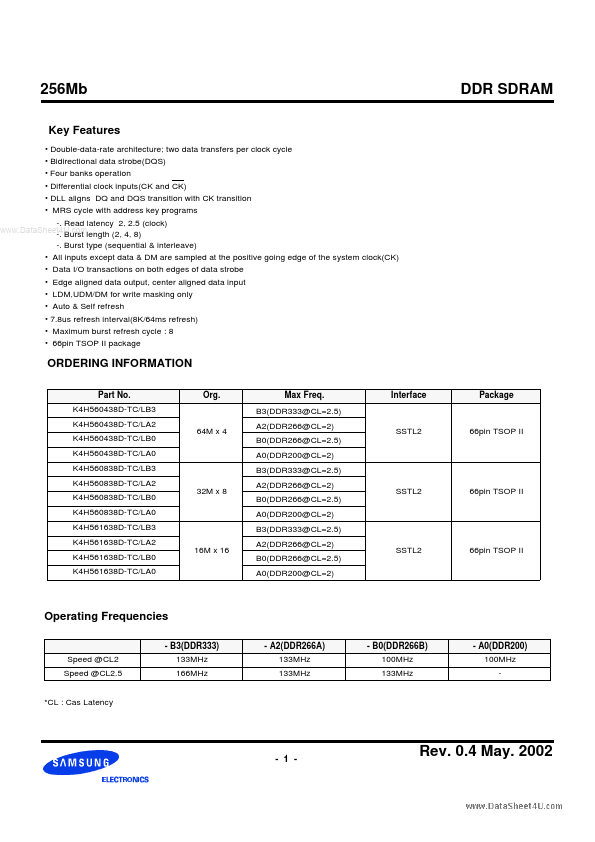
TYPE
Input
DESCRIPTION
Clock : CK and CK are differential clock inputs.All address and control input signals are sampled on the positive edge of CK and negative edge of CK.Output (read) data is referenced to both edges of CK.Internal clock signals are derived from CK/CK.Clock Enable : CKE HIGH activates, and CKE LOW deactivates internal clock signals, and device input buffers and output drivers.Deactivating the clock provides PRECHARGE POWER-DOWN and SELF REFRESH
Features
- Double-data-rate architecture; two data transfers per clock cycle.
- Bidirectional data strobe(DQS).
- Four banks operation.
- Differential clock inputs(CK and CK).
- DLL aligns DQ and DQS transition with CK transition.
- MRS cycle with address key programs -. Read latency 2, 2.5 (clock) www. DataSheet4U. com -. Burst length (2, 4, 8) -. Burst type (sequential & interleave).
- All inputs except data & DM are sampled at the positive going edge of.
 K4H560838D-TCB3_SamsungSemiconductor.pdf