Datasheet Details
- Part number
- SN74LS109A
- Manufacturer
- ON Semiconductor ↗
- File Size
- 148.97 KB
- Datasheet
- SN74LS109A_ONSemiconductor.pdf
- Description
- Dual JK Positive Edge-Triggered Flip-Flop
SN74LS109A Description
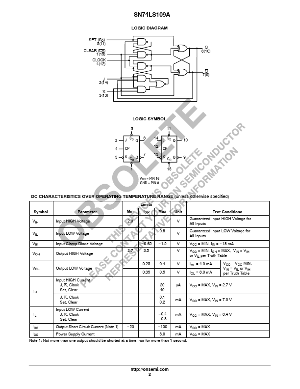
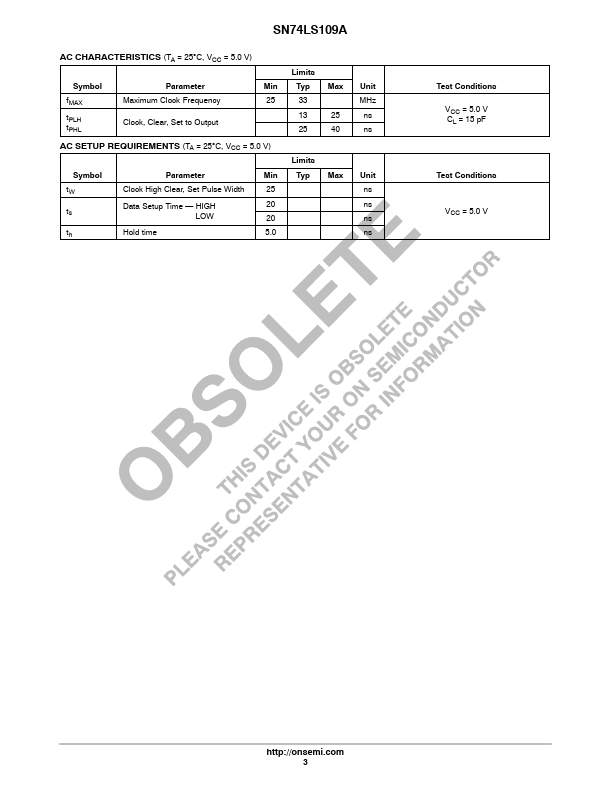
SN74LS109A Dual JK Positive Edge *Triggered Flip *Flop The SN74LS109A consists of two high speed completely independent transition clock.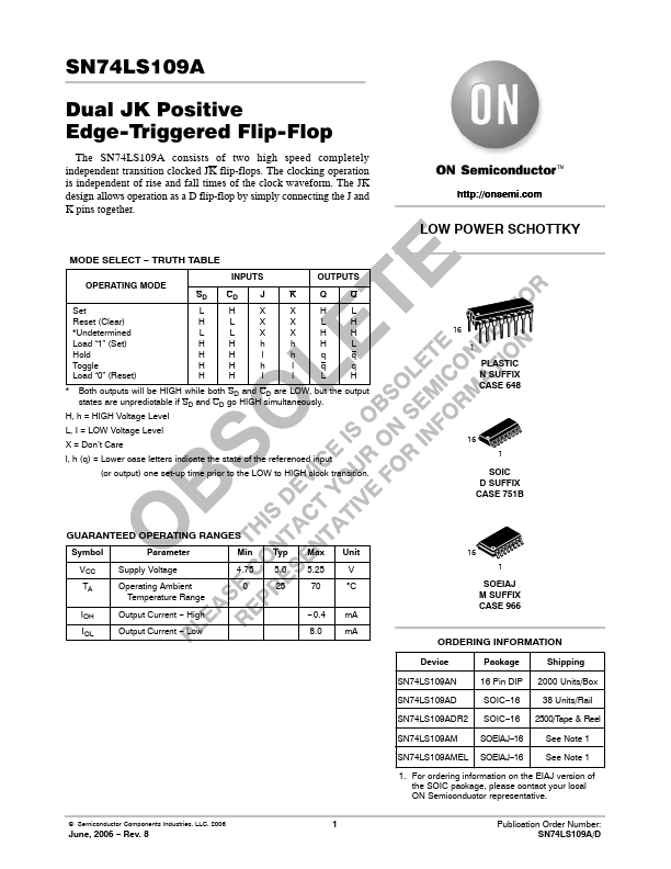
📁 Related Datasheet
📌 All Tags