Datasheet Details
| Part number | NB4N11S |
|---|---|
| Manufacturer | ON Semiconductor ↗ |
| File Size | 131.38 KB |
| Description | 3.3V 1:2 AnyLevel Input to LVDS Fanout Buffer /Translator |
| Datasheet |
 NB4N11S_ONSemiconductor.pdf NB4N11S_ONSemiconductor.pdf
|
| Part number | NB4N11S |
|---|---|
| Manufacturer | ON Semiconductor ↗ |
| File Size | 131.38 KB |
| Description | 3.3V 1:2 AnyLevel Input to LVDS Fanout Buffer /Translator |
| Datasheet |
NB4N11S_ONSemiconductor.pdf
|
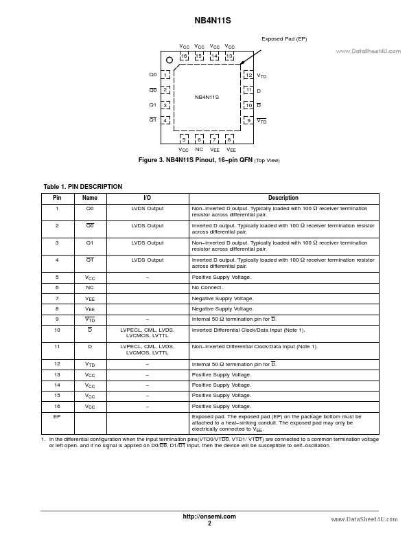
Pin 1 2 3 4 5 6 7 8 9 10 11 12 13 14 15 16 EP Name Q0 Q0 Q1 Q1 VCC NC VEE VEE VTD D D VTD VCC VCC VCC VCC LVPECL, CML, LVDS, LVCMOS, LVTTL LVPECL, CML, LVDS, LVCMOS, LVTTL I/O LVDS Output LVDS Output LVDS Output LVDS Output Description Non inverted D output.
📁 NB4N11S Similar Datasheet