Datasheet Details
| Part number | NB4N11M |
|---|---|
| Manufacturer | ON Semiconductor ↗ |
| File Size | 273.37 KB |
| Description | Multi Level Clock/Data Input to CML Receiver/Buffer/Translator |
| Datasheet |
 NB4N11M_ONSemiconductor.pdf NB4N11M_ONSemiconductor.pdf
|
| Part number | NB4N11M |
|---|---|
| Manufacturer | ON Semiconductor ↗ |
| File Size | 273.37 KB |
| Description | Multi Level Clock/Data Input to CML Receiver/Buffer/Translator |
| Datasheet |
NB4N11M_ONSemiconductor.pdf
|
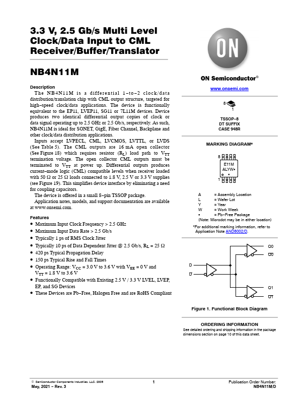
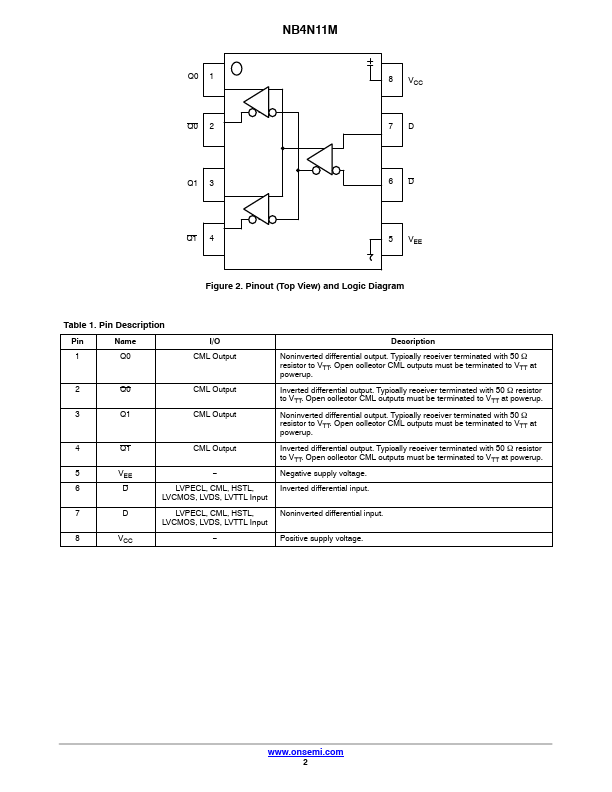
The NB4N11M is a differential 1 to 2 clock/data distribution/translation chip with CML output structure, targeted for high speed clock/data applications.
📁 NB4N11M Similar Datasheet