Datasheet4U Logo Datasheet4U.com

NB3N65027 Datasheet - ON Semiconductor

NB3N65027-ONSemiconductor.pdf

Preview of NB3N65027 PDF
NB3N65027 Datasheet Preview Page 2 NB3N65027 Datasheet Preview Page 3

Datasheet Details

Part number:

NB3N65027

Manufacturer:

ON Semiconductor ↗

File Size:

144.91 KB

Description:

3.3v programmable 3-pll clock synthesizer.

NB3N65027, 3.3V Programmable 3-PLL Clock Synthesizer

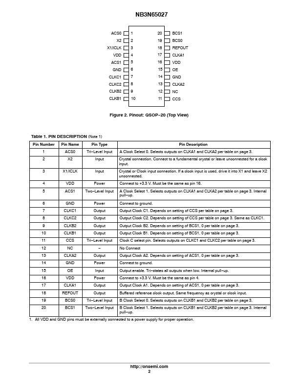
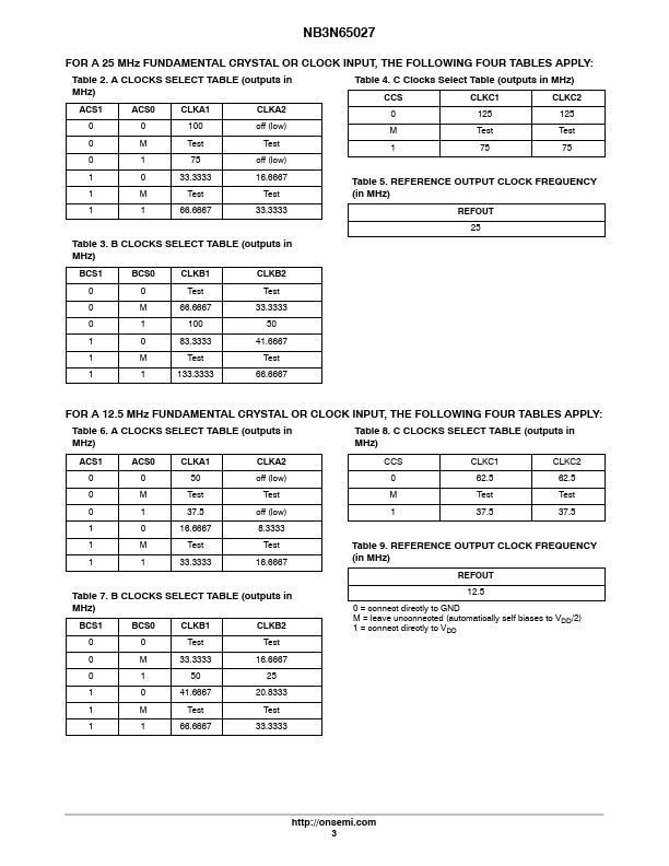
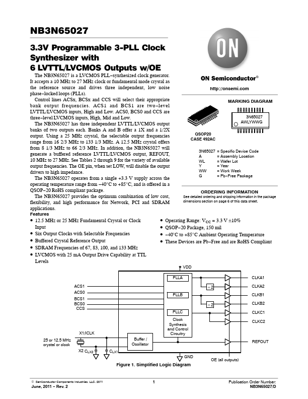
(Note 1) Pin Number Pin Name Pin Type Pin Description 1 ACS0 Tri *Level Input A Clock Select 0.

Selects outputs on CLKA1 and CLKA2 per table on page 3.

2 X2 Input Crystal connection.

Connect to a fundamental crystal or leave unconnected for a clock input.

3 X1/ICLK Input Crysta

NB3N65027 3.3V Programmable 3-PLL Clock Synthesizer with 6 LVTTL/LVCMOS Outputs w/OE The NB3N65027 is a LVCMOS PLL synthesized clock generator.

It accepts a 10 MHz to 27 MHz clock or fundamental mode crystal as the reference source and drives three independent, low noise phase locked loops (PLLs).

Control lines ACSx, BCSx and CCS will select their appropriate bank output frequencies.

ACS1 and BCS1 are two level LVTTL/LVCMOS inputs, High and Low.

ACS0, BCS0 and CCS are

NB3N65027 Features

* http://onsemi.com MARKING DIAGRAM 3N65027 AWLYWWG QSOP20 CASE 492AC 3N65027 = Specific Device Code A = Assembly Location WL = Wafer Lot Y = Year WW = Work Week G = Pb

* Free Package ORDERING INFORMATION See detailed ordering and shipping information in the package dimensions section on page 6

📁 Related Datasheet

📌 All Tags

ON Semiconductor NB3N65027-like datasheet