Datasheet4U Logo Datasheet4U.com

NB3N111K - 3.3V Differential 1:10 Fanout Clock Driver

General Description

The NB3N111K is a differential 1:10 Clock fanout buffer with High

speed Current Steering Logic (HCSL) outputs optimized for ultra low propagation delay variation.

The NB3N111K is designed with PCI Express HCSL clock distribution and FBDIMM applications in mind.

Key Features

  • Typical Input Clock Frequency 100, 133, 166, or 400 MHz.
  • 220 ps Typical Rise and Fall Times.
  • 800 ps Typical Propagation Delay.
  • Dtpd 100 ps Maximum Propagation Delay Variation per Diff Pair.
  • 0.1 ps Typical RMS Additive Phase Jitter.
  • LVDS Output Levels Optional with Interface Termination.
  • Operating Range: VCC = 3.0 V to 3.6 V with GND = 0 V.
  • Typical HCSL Output Levels (700 mV Peak.
  • to.
  • Peak).
  • LVDS Outpu.

📥 Download Datasheet

Datasheet Details

Part number NB3N111K
Manufacturer onsemi
File Size 125.17 KB
Description 3.3V Differential 1:10 Fanout Clock Driver
Datasheet download datasheet NB3N111K Datasheet

Full PDF Text Transcription (Reference)

The following content is an automatically extracted verbatim text from the original manufacturer datasheet and is provided for reference purposes only.

View original datasheet text
NB3N111K 
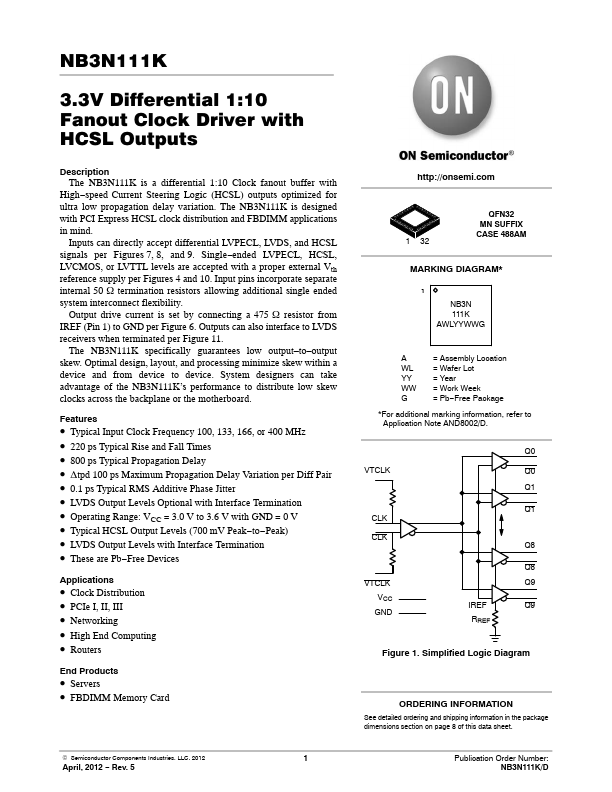
3.3V Differential 1:10 Fanout Clock Driver with HCSL Outputs Description The NB3N111K is a differential 1:10 Clock fanout buffer with High−speed Current Steering Logic (HCSL) outputs optimized for ultra low propagation delay variation. The NB3N111K is designed with PCI Express HCSL clock distribution and FBDIMM applications in mind. Inputs can directly accept differential LVPECL, LVDS, and HCSL signals per Figures 7, 8, and 9. Single−ended LVPECL, HCSL, LVCMOS, or LVTTL levels are accepted with a proper external Vth reference supply per Figures 4 and 10. Input pins incorporate separate internal 50 W termination resistors allowing additional single ended system interconnect flexibility.