Datasheet Details
| Part number | NB2870A |
|---|---|
| Manufacturer | ON Semiconductor ↗ |
| File Size | 142.36 KB |
| Description | Reduced EMI Clock Synthesizer |
| Datasheet |
 NB2870A_ONSemiconductor.pdf NB2870A_ONSemiconductor.pdf
|
| Part number | NB2870A |
|---|---|
| Manufacturer | ON Semiconductor ↗ |
| File Size | 142.36 KB |
| Description | Reduced EMI Clock Synthesizer |
| Datasheet |
NB2870A_ONSemiconductor.pdf
|
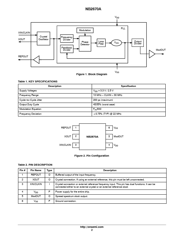
Supply Voltages Frequency Range Cycle to Cycle Jitter Output Duty Cycle Modulation Equation Frequency Deviation VDD = 3.3 V / 2.5 V VSS Specification 13 MHz < CLKIN < 30 MHz 200 ps (maximum) 45/55% (worst case) FIN/640 "0.75% (TYP) @ 22 MHz REFOUT XOUT XIN/CLKIN 1 2 3 6 VSS ModOUT VDD NB2870A 5 4 Figure 2. Pin Configuration Table 2. PIN DESCRIPTION Pin # 1 2 3 4 5 6 Pin Name REFOUT XOUT XIN/CLKIN VDD ModOUT VSS Type O O I P O P Buffered output of the input frequency.Cr
📁 NB2870A Similar Datasheet