Description
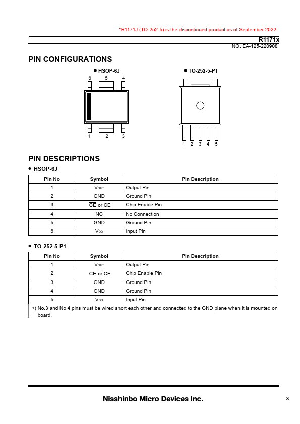
HSOP-6J
Pin No
Symbol
1
VOUT
2
GND
3
CE or CE
4
NC
5
GND
6
VDD
Output Pin Ground Pin Chip Enable Pin No Connection Ground Pin Input Pin
Pin Description
TO-252-5-P1
Pin No 1
Symbol VOUT
Output Pin
Pin Description
2
CE or CE
Chip Enable Pin
3
GND
Ground Pin
4
GND
Ground Pin
5
VDD
Input Pin
∗) No.3 and No.4 pins must be wired short each other and connected to the GND plane when it is mounted on board.3
R1171J (TO-252-5) is the discontin
Features
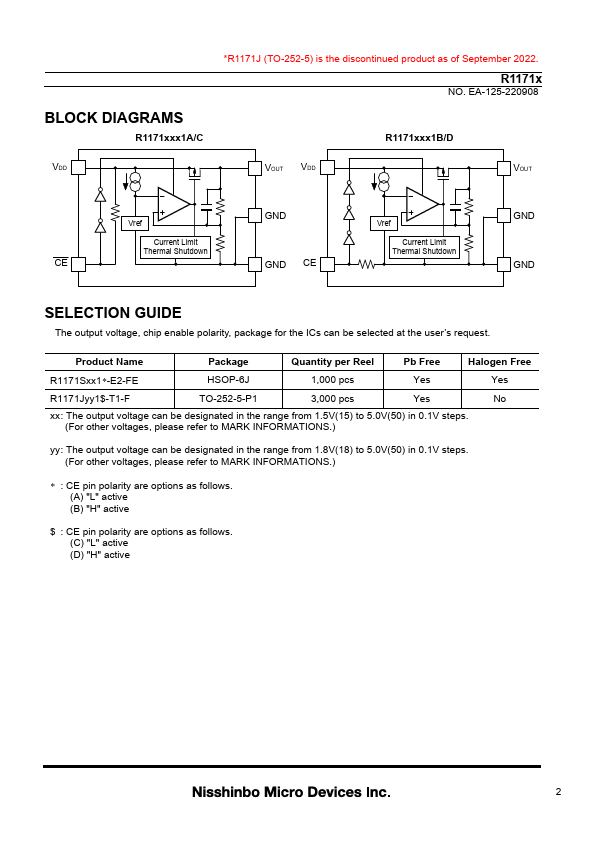
- of low dropout voltage, high output voltage accuracy, low consumption current. Each of these ICs consists of a voltage reference unit, an error amplifier, resistor net for setting output voltage, a current limit circuit at short mode, a chip enable circuit, and thermal shutdown circuit. The output voltage of R1171 is fixed in the IC. Low consumption current by the merit of CMOS process and built-in transistors with low ON-resistance make low dropout voltage and chip enable function prolongs the.
 R1171S-Nisshinbo.pdf