The following content is an automatically extracted verbatim text
from the original manufacturer datasheet and is provided for reference purposes only.
View original datasheet text
SEMICONDUCTOR
TECHNICAL DATA
GENERAL PURPOSE APPLICATION. SWITCHING APPLICATION.
FEATURES Complementary to BCW29/30.
MAXIMUM RATING (Ta=25 )
CHARACTERISTIC
SYMBOL RATING
Collector-Base Voltage Collector-Emitter Voltage Emitter-Base Voltage Collector Current Collector Power Dissipation Junction Temperature
VCBO VCEO VEBO
IC PC * Tj
30 20 5 100 350 150
Storage Temperature Range
Tstg -55 150
* : Package Mounted On 99.9% Alumina 10 8 0.6mm.
UNIT V V V mA mW
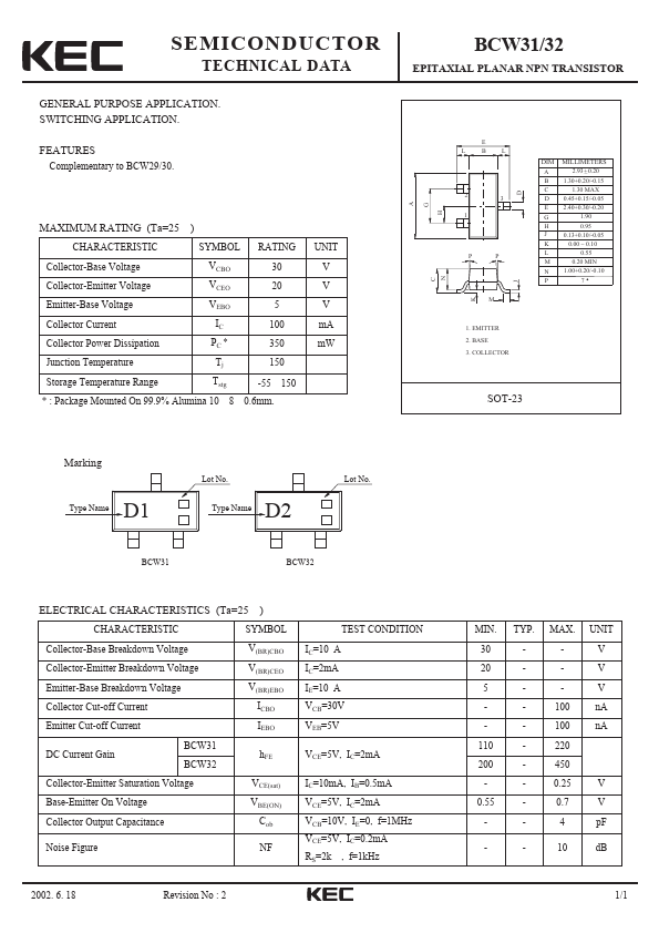
A G H
D
BCW31/32
EPITAXIAL PLANAR NPN TRANSISTOR
E L BL
23 1
PP
M 1. EMITTER 2. BASE 3. COLLECTOR
DIM A B C D E G H J
K L M
N P
MILLIMETERS 2.93+_ 0.20
1.30+0.20/-0.15
1.30 MAX 0.45+0.15/-0.05 2.40+0.30/-0.20
1.90 0.95 0.13+0.10/-0.05 0.00 ~ 0.10 0.55 0.20 MIN
1.00+0.20/-0.10 7
SOT-23
C N K J
Marking
D1Type Name
Lot No.
 BCW31 Datasheet