Datasheet Details
| Part number | 2N3864 |
|---|---|
| Manufacturer | Inchange Semiconductor |
| File Size | 178.57 KB |
| Description | NPN Transistor |
| Datasheet |
 2N3864 Datasheet 2N3864 Datasheet
|
|
|
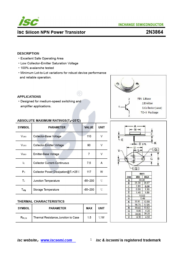
and reliable operation.
amplifier applications.
| Part number | 2N3864 |
|---|---|
| Manufacturer | Inchange Semiconductor |
| File Size | 178.57 KB |
| Description | NPN Transistor |
| Datasheet |
2N3864 Datasheet
|
|
|
|