Datasheet4U Logo Datasheet4U.com

GS8342Q36BD-250 - 36Mb SigmaQuad-II Burst of 2 SRAM

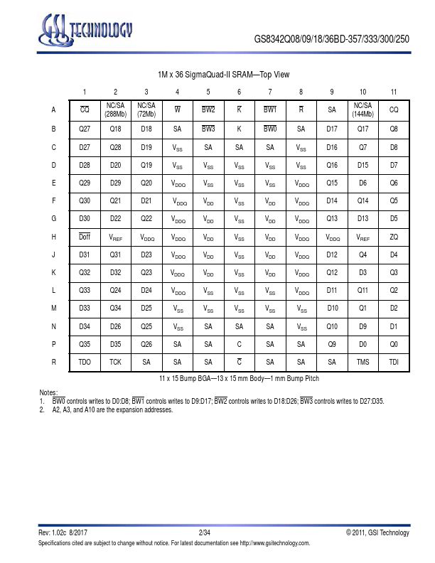
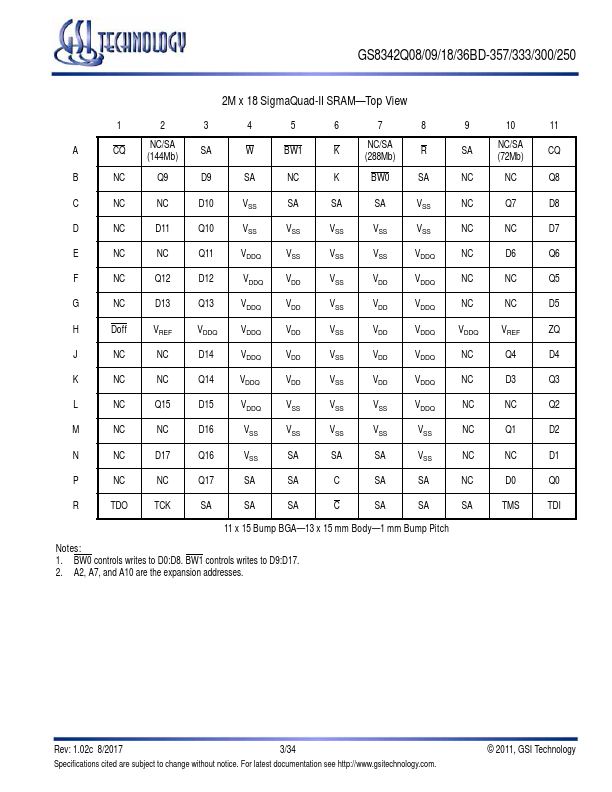
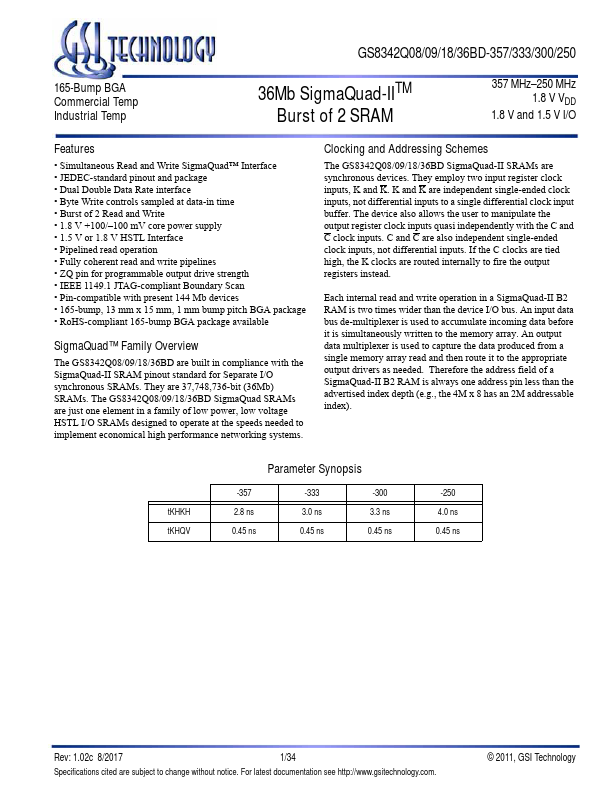
This page provides the datasheet information for the GS8342Q36BD-250, a member of the GS8342Q08 36Mb SigmaQuad-II Burst of 2 SRAM family.

Datasheet Summary

Features

  • Simultaneous Read and Write SigmaQuad™ Interface.
  • JEDEC-standard pinout and package.
  • Dual Double Data Rate interface.
  • Byte Write controls sampled at data-in time.
  • Burst of 2 Read and Write.
  • 1.8 V +100/.
  • 100 mV core power supply.
  • 1.5 V or 1.8 V HSTL Interface.
  • Pipelined read operation.
  • Fully coherent read and write pipelines.
  • ZQ pin for programmable output drive strength.
  • IEEE 1149.1 JTAG-co.

📥 Download Datasheet

Datasheet preview – GS8342Q36BD-250

Datasheet Details

Part number GS8342Q36BD-250
Manufacturer GSI Technology
File Size 660.69 KB
Description 36Mb SigmaQuad-II Burst of 2 SRAM
Datasheet download datasheet GS8342Q36BD-250 Datasheet
Additional preview pages of the GS8342Q36BD-250 datasheet.
Other Datasheets by GSI Technology

Full PDF Text Transcription

Click to expand full text
GS8342Q08/09/18/36BD-357/333/300/250 165-Bump BGA Commercial Temp Industrial Temp 36Mb SigmaQuad-IITM Burst of 2 SRAM 357 MHz–250 MHz 1.8 V VDD 1.8 V and 1.5 V I/O Features • Simultaneous Read and Write SigmaQuad™ Interface • JEDEC-standard pinout and package • Dual Double Data Rate interface • Byte Write controls sampled at data-in time • Burst of 2 Read and Write • 1.8 V +100/–100 mV core power supply • 1.5 V or 1.8 V HSTL Interface • Pipelined read operation • Fully coherent read and write pipelines • ZQ pin for programmable output drive strength • IEEE 1149.
Published: |