Datasheet Details
| Part number | GS8342Q36E-200 |
|---|---|
| Manufacturer | GSI Technology |
| File Size | 865.00 KB |
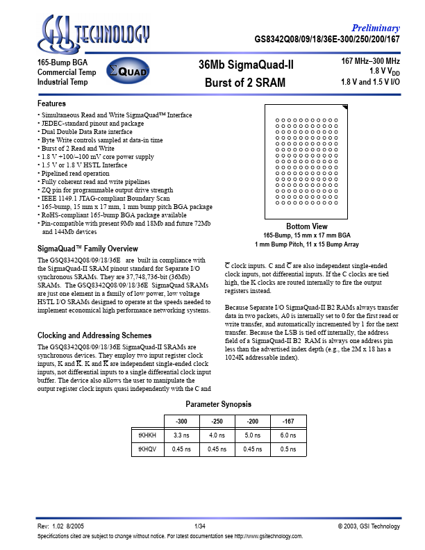
| Description | 36Mb SigmaQuad-II Burst of 2 SRAM |
| Datasheet |
 GS8342Q36E-200 Datasheet GS8342Q36E-200 Datasheet
|
|
|
Download the GS8342Q36E-200 datasheet PDF. This datasheet also covers the GS8342Q08E-300 variant, as both devices belong to the same 36mb sigmaquad-ii burst of 2 sram family and are provided as variant models within a single manufacturer datasheet.
| Part number | GS8342Q36E-200 |
|---|---|
| Manufacturer | GSI Technology |
| File Size | 865.00 KB |
| Description | 36Mb SigmaQuad-II Burst of 2 SRAM |
| Datasheet |
GS8342Q36E-200 Datasheet
|
|
|
|
| Part Number | Description | Manufacturer |
|---|---|---|
| GS8331 | 350KHZ Zero-Drift CMOS Rail-to-Rail IO Opamp | GAINSIL |
| GS8332 | 350KHZ Zero-Drift CMOS Rail-to-Rail IO Opamp | GAINSIL |
| GS8334 | 350KHZ Zero-Drift CMOS Rail-to-Rail IO Opamp | GAINSIL |
| GS8000 | DVI / HDMI Extender | Gennum Corporation |
| GS8041 | 14.5KHZ CMOS Rail-to-Rail I/O Opamp | GAINSIL |
| Part Number | Description |
|---|---|
| GS8342Q36E-250 | 36Mb SigmaQuad-II Burst of 2 SRAM |
| GS8342Q36E-167 | 36Mb SigmaQuad-II Burst of 2 SRAM |
| GS8342Q36E-300 | 36Mb SigmaQuad-II Burst of 2 SRAM |
| GS8342Q36AE | 36Mb SigmaQuad-II Burst of 2 SRAM |
| GS8342Q36BD-250 | 36Mb SigmaQuad-II Burst of 2 SRAM |