Description
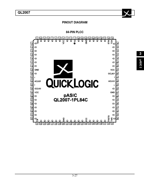
Pin TDI TRSTB TMS TCK TDO STM I/ACLK I/GCLK I I/O VCC GND Function Test Data In for JTAG Active low Reset for JTAG Test Mode Select for JTAG Test Clock for JTAG Test data out for JTAG Special Test Mode High-drive input and/or array network driver High-drive input and/or global network driver High-drive input Input/Output pin Power supply pin Ground pin Description Hold HIGH during normal operation.
Features
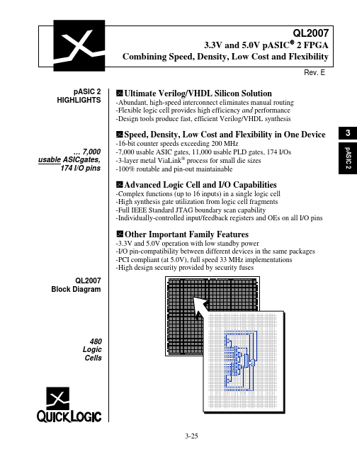
- -3.3V and 5.0V operation with low standby power -I/O pin-compatibility between different devices in the same packages -PCI compliant (at 5.0V), full speed 33 MHz implementations -High design security provided by security fuses QL2007 Block Diagram
480 Logic Cells
3-25
DataSheet 4 U . com
www. DataSheet4U. com
QL2007.
 QL2007_ETC.pdf