Datasheet4U Logo Datasheet4U.com

CY7C1041V33 - 256K x 16 Static RAM

Datasheet Summary

Description

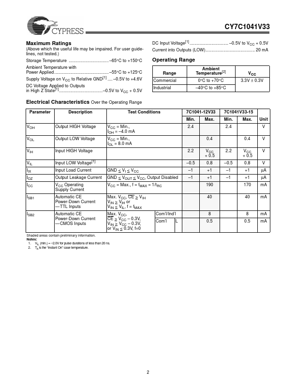
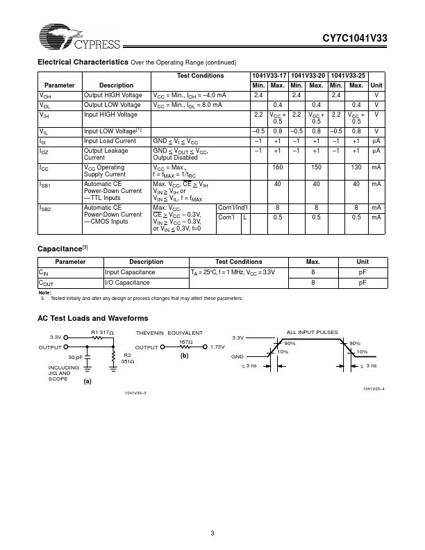
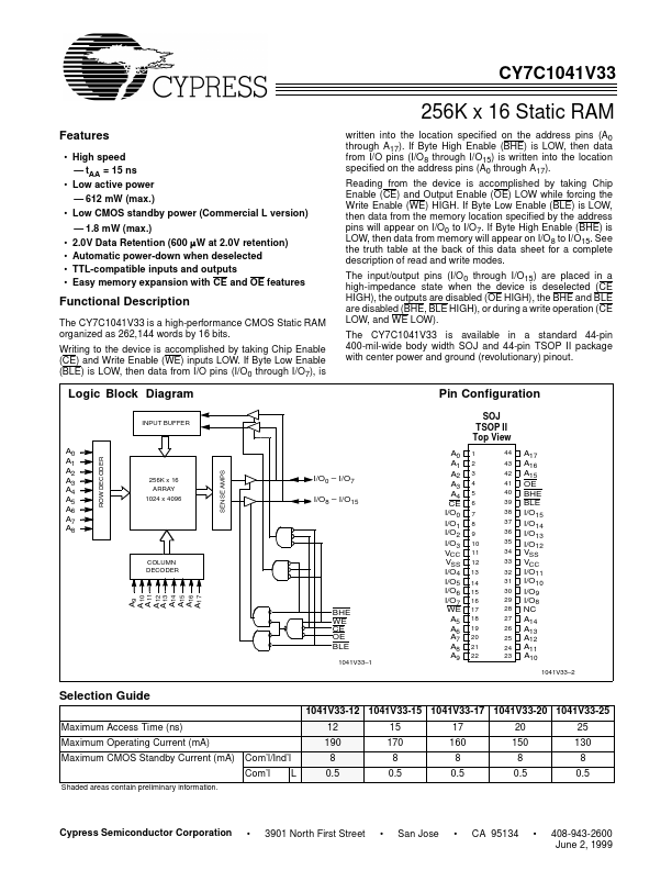
of read and write modes.

The input/output pins (I/O 0 through I/O15) are placed in a high-impedance state when the device is deselected (CE HIGH), the outputs are disabled (OE HIGH), the BHE and BLE are disabled (BHE, BLE HIGH), or during a write operation (CE LOW, and WE LOW).

Features

  • High speed.
  • tAA = 15 ns.
  • Low active power.
  • 612 mW (max. ).
  • Low CMOS standby power (Commercial L version).
  • 1.8 mW (max. ).
  • 2.0V Data Retention (600 µ W at 2.0V retention).
  • Automatic power-down when deselected.
  • TTL-compatible inputs and outputs.
  • Easy memory expansion with CE and OE features written into the location specified on the address pins (A0 through A17). If Byte High Enable (BHE) is LOW, then data fro.

📥 Download Datasheet

Datasheet preview – CY7C1041V33

Datasheet Details

Part number CY7C1041V33
Manufacturer Cypress Semiconductor
File Size 180.86 KB
Description 256K x 16 Static RAM
Datasheet download datasheet CY7C1041V33 Datasheet
Additional preview pages of the CY7C1041V33 datasheet.
Other Datasheets by Cypress Semiconductor

Full PDF Text Transcription

Click to expand full text
V33 CY7C1041V33 256K x 16 Static RAM Features • High speed — tAA = 15 ns • Low active power — 612 mW (max.) • Low CMOS standby power (Commercial L version) — 1.8 mW (max.) • 2.0V Data Retention (600 µ W at 2.0V retention) • Automatic power-down when deselected • TTL-compatible inputs and outputs • Easy memory expansion with CE and OE features written into the location specified on the address pins (A0 through A17). If Byte High Enable (BHE) is LOW, then data from I/O pins (I/O 8 through I/O15) is written into the location specified on the address pins (A0 through A17). Reading from the device is accomplished by taking Chip Enable (CE) and Output Enable (OE) LOW while forcing the Write Enable (WE) HIGH.
Published: |