Datasheet4U Logo Datasheet4U.com

CY2PP326 - 2 x 2 Clock and Data Switch Buffer

Description

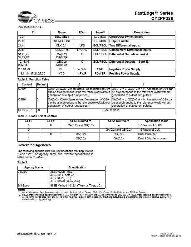
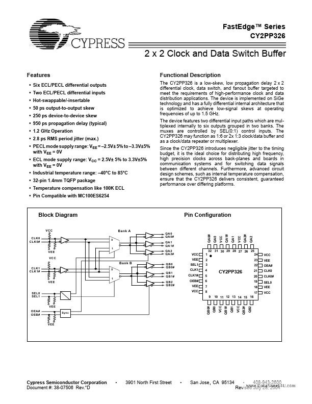
The CY2PP326 is a low-skew, low propagation delay 2 x 2 differential clock, data switch, and fanout buffer targeted to meet the requirements of high-performance clock and data distribution applications.

Features

  • Six ECL/PECL differential outputs.
  • Two ECL/PECL differential inputs.
  • Hot-swappable/-insertable.
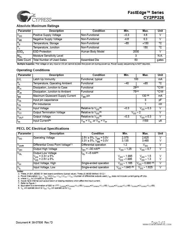
  • 50 ps output-to-output skew.
  • 250 ps device-to-device skew.
  • 950 ps propagation delay (typical).
  • 1.2 GHz Operation.
  • 2.8 ps RMS period jitter (max. ).
  • PECL mode supply range: VEE =.
  • 2.5V± 5% to.
  • 3.3V±5% with VEE = 0V.
  • ECL mode supply range: VCC = 2.5V± 5% to 3.3V±5% with VEE = 0V.
  • Industrial.

📥 Download Datasheet

Other Datasheets by Cypress Semiconductor

Full PDF Text Transcription

Click to expand full text
FastEdge™ Series CY2PP326 www.DataSheet4U.com 2 x 2 Clock and Data Switch Buffer Features • Six ECL/PECL differential outputs • Two ECL/PECL differential inputs • Hot-swappable/-insertable • 50 ps output-to-output skew • 250 ps device-to-device skew • 950 ps propagation delay (typical) • 1.2 GHz Operation • 2.8 ps RMS period jitter (max.) • PECL mode supply range: VEE = –2.5V± 5% to –3.3V±5% with VEE = 0V • ECL mode supply range: VCC = 2.5V± 5% to 3.3V±5% with VEE = 0V • Industrial temperature range: –40°C to 85°C • 32-pin 1.
Published: |