Datasheet Details
| Part number | CY2PD817 |
|---|---|
| Manufacturer | Cypress (Infineon) |
| File Size | 84.81 KB |
| Description | PECL/CMOS Buffer |
| Datasheet |
 CY2PD817 Datasheet CY2PD817 Datasheet
|
|
|
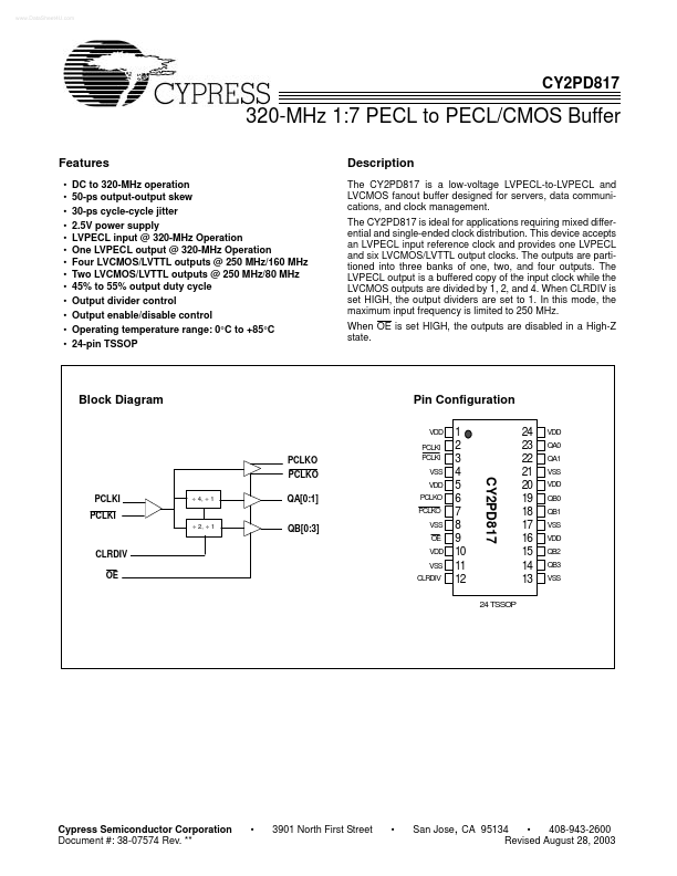
The CY2PD817 is a low-voltage LVPECL-to-LVPECL and LVCMOS fanout buffer designed for servers, data communications, and clock management.
The CY2PD817 is ideal for applications requiring mixed differential and single-ended clock distribution.
| Part number | CY2PD817 |
|---|---|
| Manufacturer | Cypress (Infineon) |
| File Size | 84.81 KB |
| Description | PECL/CMOS Buffer |
| Datasheet |
CY2PD817 Datasheet
|
|
|
|
| Part Number | Description | Manufacturer |
|---|---|---|
| CY20AAJ-8F | Nch IGBT for STROBE FLASHER | Powerex Power Semiconductors |
| CY20AAJ-8H | N Channel IGBT | Renesas |
| CY20APS | Quartz Crystal Low Profile HC49S Leaded Crystal | Crystek Corporation |
| CY20APSMD | Quartz Crystal Surface Mount HC49S SMD Crystal | Crystek Corporation |
| CY20AS | Quartz Crystal Low Profile HC49S Leaded Crystal | Crystek Corporation |
| Part Number | Description |
|---|---|
| CY2PP3115 | Differential Fanout Buffer |
| CY2PP3210 | Dual 1:5 Differential Clock / Data Fanout Buffer |
| CY2PP3220 | Dual 1:10 Differential Clock / Data Fanout Buffer |
| CY2PP326 | 2 x 2 Clock and Data Switch Buffer |
| CY2037 | High Accuracy EPROM Programmable PLL Die for Crystal Oscillators |
The following content is an automatically extracted verbatim text from the original manufacturer datasheet and is provided for reference purposes only.