Description
10
1.1 Device overview 10 1.2 Block diagram 13 2. Pinouts and pin descriptions 14 2.1 Pinouts 14
2.1.1 A31G323RLN, A31G324RLN (64 LQFP) 14 2.1.2 A31G323CLN, A31G324CLN (48 LQFP) 15 2.1.3 A31G323CUN, A31G324CUN (48 QFN) 16 2.2 Pin description 17 3. System and memory overview 26 3.1 System architecture 26 3.1.1 Cortex-M0+ Core 26 3.1.2 Interrupt controller 26 3.2 Memory organization 29 3.2.1 Register boundary address 29 3.2.2 Memory map 30 3.2.3 Embedded SRAM
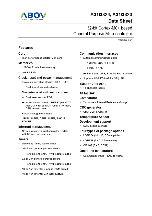
Features
- Core.
- High performance Cortex-M0+ core
Memories.
- 128/64KB code flash memory.
- 16KB SRAM
Clock, reset and power management.
- Two main operating clocks: HCLK, PCLK.
- Real time clock and calendar.
- Two system reset: cold reset, warm reset.
- Cold reset source: POR.
- Warm reset sources: nRESET pin, WDT reset, LVR reset, MON reset, S/W reset, CPU request reset
Power management mode : RUN, SLEEP, DEEP SLEEP, BAKUP POWER
Interrupt management.
- Nested vec.
 A31G323 Datasheet