TH50VSF3583AASB
TH50VSF3583AASB is MULTI-CHIP INTEGRATED CIRCUIT SILICON GATE CMOS manufactured by Toshiba.
- Part of the TH50VSF3582AASB comparator family.
- Part of the TH50VSF3582AASB comparator family.
DESCRIPTION
The TH50VSF3582/3583AASB is a mixed multi-chip package containing a 8,388,608-bit Full CMOS SRAM and a 33,554,432-bit flash memory. The CIOS and CIOF inputs can be used to select the optimal memory configuration. The power supply. FLASH MEMORY a Simultaneous Read/Write operation so that data can be read during a Write or Erase operation. The TH50VSF3582/3583AASB can range from 2.67 V to 3.3 V. The TH50VSF3582/3583AASB is available in a 69-pin BGA package, making it suitable for a variety of design applications.
FEATURES
Power supply voltage VCCs = 2.67 V~3.3 V VCCf = 2.67 V~3.3 V ..
- Data retention supply voltage VCCs = 1.5 V~3.3 V
- Current consumption Operating: 45 m A maximum (CMOS level) Standby: 10 µA maximum (SRAM CMOS level) Standby: 10 µA maximum (FLASH)
- Block erase architecture for flash memory 8 × 8 Kbytes 63 × 64 Kbytes
- Organization
- CIOF VCC VCC VSS CIOS VCC VSS VSS Flash Memory 2,097,152 words of 16 bits 2,097,152 words of 16 bits 4,194,304 words of 8 bits SRAM 524,288 words of 16 bits 1,048,576 words of 8 bits 1,048,576 words of 8 bits
- -
- -
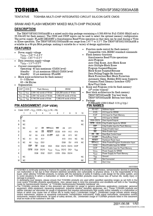
- PIN ASSIGNMENT (TOP VIEW)
- Case: CIOF = VCC, CIOS = VCC (×16, ×16)
1 2 3 4 5 6 7 8 9 10
Function mode control for flash memory patible with JEDEC-standard mands Flash memory functions Simultaneous Read/Write operations Auto-Program Auto Chip Erase, Auto Block Erase Auto Multiple-Block Erase Program Suspend/Resume Block-Erase Suspend/Resume Data Polling/Toggle Bit function Block Protection/Boot Block Protection Automatic Sleep, Hidden ROM Area Supports mon Flash Memory Interface (CFI) Byte/Word Mode Erase and Program cycle for flash memory 105 cycles (typical) Boot block architecture for flash memory TH50VSF3582AASB: Top boot block TH50VSF3583AASB: Bottom boot block Package P-FBGA69-1209-0.80A3: 0.31 g (typ.)
PIN NAMES
A0~A21 A12S A12F SA DQ0~DQ15 CEF OE
Address Inputs A12 Input for SRAM A12 Input for Flash Memory A18 Input for SRAM Data Inputs/Outputs Chip Enable Input for Flash Memory...