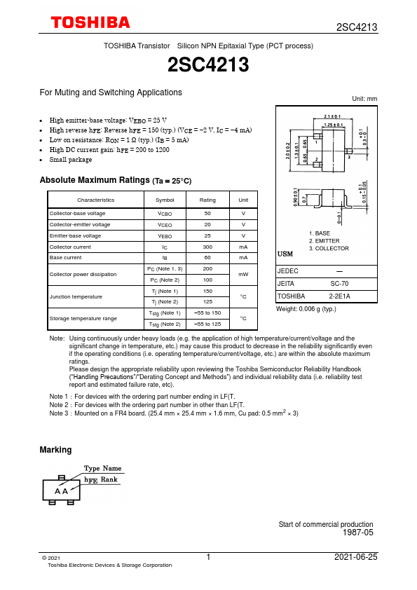
TOSHIBA Transistor Silicon NPN Epitaxial Type (PCT process)
2SC4213
2SC4213
For Muting and Switching Applications
Unit: mm
• High emitter-base voltage: VEBO = 25 V (min)
• High reverse hFE: Reverse hFE = 150 (typ.) (VCE = −2 V, IC = −4 mA)
• Low on resistance: RON = 1 Ω (typ.) (IB = 5 mA)
• High DC current gain: hFE = 200~1200
• Small package
Absolute Maximum Ratings (Ta = 25°C)
Characteristics
Symbol
Rating
Unit
Collector-base voltage
VCBO 50 V
Collector-emitter voltage
VCEO 20 V
Emitter-base voltage
VEBO 25 V
Collector current
IC 300 mA
Base current
IB 60 mA
Collector power dissipation
PC
100 mW
JEDEC
―
Junction temperature
Storage temperature range
Tj 125 °C
Tstg
−55~125
°C
JEITA
TOSHIBA
SC-70
2-2E1A
Note: Using continuously under heavy loads (e.g. the application of high
temperature/current/voltage and the significant change in
Weight: 0.006 g (typ.)
temperature, etc.) may cause this product to decrease in the
reliability significantly even if the operating conditions (i.e. operating temperature/current/voltage, etc.) are
within the absolute maximum ratings.
Please design the appropriate reliability upon reviewing the Toshiba Semiconductor Reliability Handbook
(“Handling Precautions”/“Derating Concept and Methods”) and individual reliability data (i.e. reliability test
report and estimated failure rate, etc).
Marking
1 2007-11-01