Datasheet Details
| Part number | K4T51043Q |
|---|---|
| Manufacturer | Samsung Semiconductor |
| File Size | 507.78 KB |
| Description | 512Mb B-die DDR2 SDRAM |
| Datasheet |
 K4T51043Q Datasheet K4T51043Q Datasheet
|
|
|
3.
4.
Rev.
| Part number | K4T51043Q |
|---|---|
| Manufacturer | Samsung Semiconductor |
| File Size | 507.78 KB |
| Description | 512Mb B-die DDR2 SDRAM |
| Datasheet |
K4T51043Q Datasheet
|
|
|
|
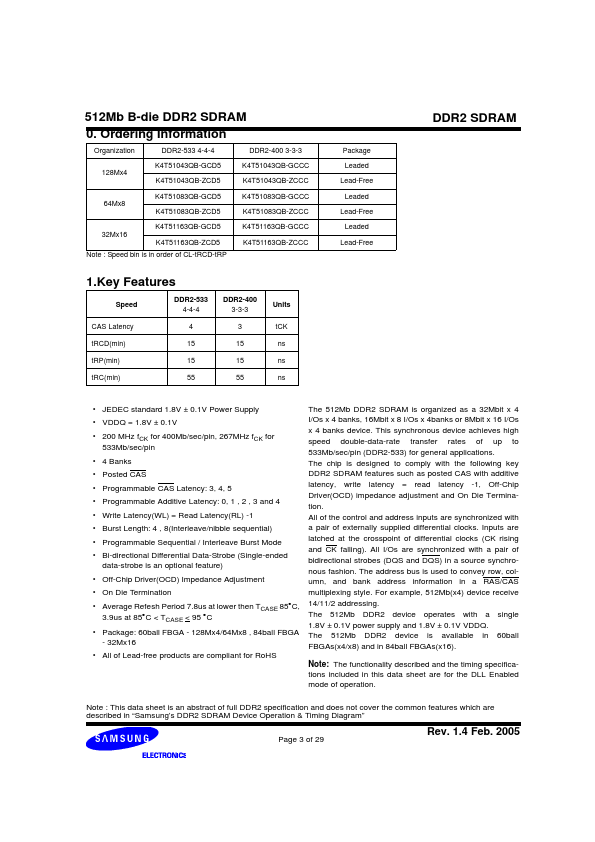
| Part Number | Description | Manufacturer |
|---|---|---|
| K4T51043QB-GCD5 | 512Mb B-die DDR2 SDRAM | Samsung semiconductor |
| K4T51043QB-ZCD5 | 512Mb B-die DDR2 SDRAM | Samsung semiconductor |
| K4T51043QE | 512Mb E-die DDR2 SDRAM Specification | Samsung semiconductor |
| K4T51083QB-GCD5 | 512Mb B-die DDR2 SDRAM | Samsung semiconductor |
| K4T51083QB-ZCD5 | 512Mb B-die DDR2 SDRAM | Samsung semiconductor |
| Part Number | Description |
|---|---|
| K4T51043QG | 512Mb G-die DDR2 SDRAM |
| K4T51043QI | 512Mb I-die DDR2 SDRAM |
| K4T51043QJ | 512Mb J-die DDR2 SDRAM |
| K4T51083QC | 512Mb C-die DDR2 SDRAM |
| K4T51083QG | 512Mb G-die DDR2 SDRAM |
The following content is an automatically extracted verbatim text from the original manufacturer datasheet and is provided for reference purposes only.