STN8205A
STN8205A is 5A Dual N-Channel Enhancement Mode MOSFET manufactured by STANSON.
DESCRIPTION
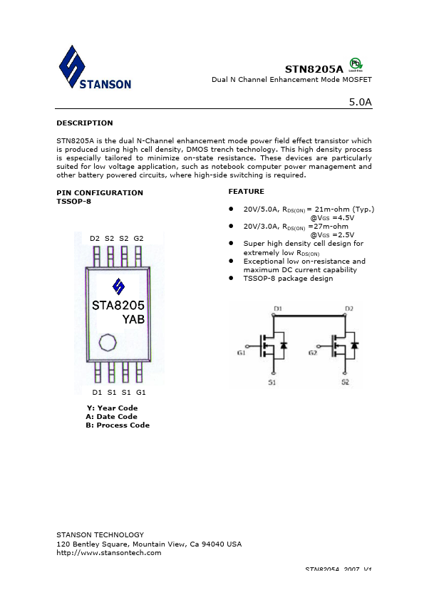
STN8205A is the dual N-Channel enhancement mode power field effect transistor which is produced using high cell density, DMOS trench technology. This high density process is especially tailored to minimize on-state resistance. These devices are particularly suited for low voltage application, such as notebook puter power management and other battery powered circuits, where high-side switching is required.
PIN CONFIGURATION TSSOP-8
D2 S2 S2 G2
FEATURE l 20V/5.0A, RDS(ON) = 21m-ohm (Typ.) @VGS =4.5V l 20V/3.0A, RDS(ON) =27m-ohm @VGS =2.5V l Super high density cell design for extremely low RDS(ON) l Exceptional low on-resistance and maximum DC current capability l TSSOP-8 package design
D1 S1 S1 G1
Y: Year Code A: Date Code B: Process Code
STANSON TECHNOLOGY 120 Bentley Square, Mountain View, Ca 94040 USA http://.stansontech.
STN8205A 2007. V1
Dual N Channel Enhancement Mode MOSFET
5.0A
ABSOULTE MAXIMUM RATINGS (Ta = 25℃ unless otherwise noted )
Parameter
Symbol
Typical
Drain-Source Voltage
Gate-Source Voltage
Continuous Drain Current (TJ=150℃) TA=25℃ TA=70℃
Pulsed Drain Current
Continuous Source Current (Diode Conduction)
Power Dissipation
TA=25℃ TA=70℃
Operation Junction Temperature Storage Temperature Range Thermal Resistance-Junction to Ambient
VDSS VGSS
IDM IS PD
TJ TSTG RθJA
20 +/-20
5.0 3.4 30
2 2.0 1.2 -40/140 -55/150 105
Unit V V A
℃ ℃ ℃/W
STANSON TECHNOLOGY 120 Bentley Square, Mountain View, Ca 94040 USA http://.stansontech.
STN8205A 2007. V1
Dual N Channel Enhancement Mode MOSFET
5.0A
ELECTRICAL CHARACTERISTICS ( Ta = 25℃ unless otherwise noted )
Parameter
Static...