Datasheet Details
| Part number | 9FGL0841D |
|---|---|
| Manufacturer | Renesas Electronics |
| File Size | 1.39 MB |
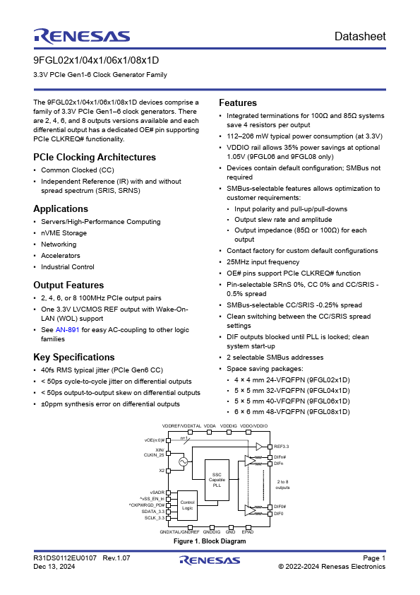
| Description | 3.3V PCIe Gen1-6 Clock Generator |
| Datasheet |
 9FGL0841D Datasheet 9FGL0841D Datasheet
|
|
|
Download the 9FGL0841D datasheet PDF (9FGL0241D included). The manufacturer datasheet provides complete specifications, pinout details, electrical characteristics, and typical applications for 3.3v pcie gen1-6 clock generator.
2.
.
| Part number | 9FGL0841D |
|---|---|
| Manufacturer | Renesas Electronics |
| File Size | 1.39 MB |
| Description | 3.3V PCIe Gen1-6 Clock Generator |
| Datasheet |
9FGL0841D Datasheet
|
|
|
|