Datasheet Details
| Part number | 9FGL0441 |
|---|---|
| Manufacturer | Renesas |
| File Size | 1.32 MB |
| Description | 3.3V PCIe Gen1-5 Clock Generator |
| Datasheet |
 9FGL0441 Datasheet 9FGL0441 Datasheet
|
|
|
This page provides the datasheet information for the 9FGL0441, a member of the 9FGL0241 3.3V PCIe Gen1-5 Clock Generator family.
5 clock generators.
There are 2, 4, 6 and 8 outputs versions available and each differential output has a dedicated OE# pin supporting PCIe CLKREQ# functionality.
Common Clocked (CC)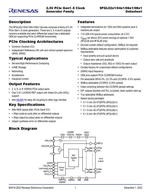
| Part number | 9FGL0441 |
|---|---|
| Manufacturer | Renesas |
| File Size | 1.32 MB |
| Description | 3.3V PCIe Gen1-5 Clock Generator |
| Datasheet |
9FGL0441 Datasheet
|
|
|
|