Datasheet4U Logo Datasheet4U.com

FDY1002PZ - Dual P-Channel MOSFET

Description

These P Channel Logic Level MOSFETs are produced using onsemi’s advanced POWERTRENCH process that has been especially tailored to minimize the on

state resistance and yet maintain low gate charge for superior switching performance.

Features

  • Max rDS(on) = 0.5 W at VGS =.
  • 4.5 V, ID =.
  • 0.83 A.
  • Max rDS(on) = 0.7 W at VGS =.
  • 2.5 V, ID =.
  • 0.70 A.
  • Max rDS(on) = 1.2 W at VGS =.
  • 1.8 V, ID =.
  • 0.43 A.
  • Max rDS(on) = 1.8 W at VGS =.
  • 1.5 V, ID =.
  • 0.36 A.
  • HBM ESD Protection Level = 1400 V (Note 1).
  • This Device is Pb.
  • Free and is RoHS Compliant.

📥 Download Datasheet

Datasheet Details

Part number FDY1002PZ
Manufacturer onsemi
File Size 251.05 KB
Description Dual P-Channel MOSFET
Datasheet download datasheet FDY1002PZ Datasheet
Other Datasheets by ON Semiconductor

Full PDF Text Transcription

Click to expand full text
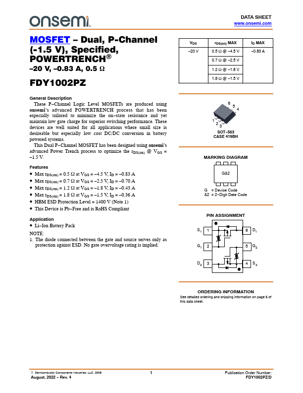
MOSFET – Dual, P-Channel (-1.5 V), Specified, POWERTRENCH) –20 V, –0.83 A, 0.5 W FDY1002PZ General Description These P−Channel Logic Level MOSFETs are produced using onsemi’s advanced POWERTRENCH process that has been especially tailored to minimize the on−state resistance and yet maintain low gate charge for superior switching performance. These devices are well suited for all applications where small size is desireable but especially low cost DC/DC conversion in battery powered systems. This Dual P−Channel MOSFET has been designed using onsemi’s advanced Power Trench process to optimize the rDS(on) @ VGS = –1.5 V. Features • Max rDS(on) = 0.5 W at VGS = –4.5 V, ID = –0.83 A • Max rDS(on) = 0.7 W at VGS = –2.5 V, ID = –0.70 A • Max rDS(on) = 1.2 W at VGS = –1.8 V, ID = –0.
Published: |