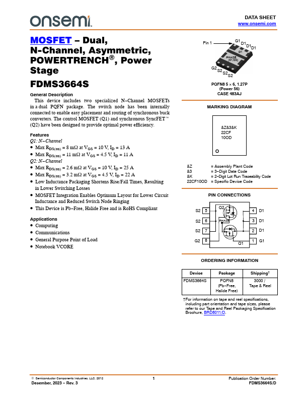
FDMS3664S
Overview
This device includes two specialized N-Channel MOSFETs in a dual PQFN package. The switch node has been internally connected to enable easy placement and routing of synchronous buck converters.
- Max RDS(on) = 8 mW at VGS = 10 V, ID = 13 A
- Max RDS(on) = 11 mW at VGS = 4.5 V, ID = 11 A Q2: N-Channel
- Max RDS(on) = 2.6 mW at VGS = 10 V, ID = 25 A
- Max RDS(on) = 3.2 mW at VGS = 4.5 V, ID = 22 A
- Low Inductance Packaging Shortens Rise/Fall Times, Resulting in Lower Switching Losses
- MOSFET Integration Enables Optimum Layout for Lower Circuit Inductance and Reduced Switch Node Ringing
- This Device is Pb-Free, Halide Free and is RoHS Compliant