Datasheet Details
| Part number | BFR31 |
|---|---|
| Manufacturer | Motorola Semiconductor (now NXP Semiconductors) |
| File Size | 30.97 KB |
| Description | JFET |
| Datasheet |
 BFR31 Datasheet BFR31 Datasheet
|
|
|
|
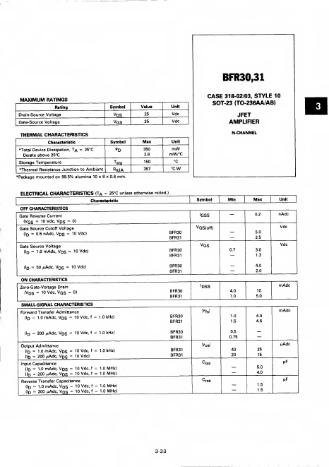
Download the BFR31 datasheet PDF. This datasheet also covers the BFR30 variant, as both devices belong to the same jfet family and are provided as variant models within a single manufacturer datasheet.
| Part number | BFR31 |
|---|---|
| Manufacturer | Motorola Semiconductor (now NXP Semiconductors) |
| File Size | 30.97 KB |
| Description | JFET |
| Datasheet |
BFR31 Datasheet
|
|
|
|
| Part Number | Description | Manufacturer |
|---|---|---|
| BFR31 | N-channel field-effect transistors | NXP |
| BFR31LT1 | JFET Amplifiers | Motorola Inc |
| BFR31LT1 | JFET Amplifiers | ON Semiconductor |
| BFR30 | N-channel field-effect transistors | NXP |
| BFR30LT1 | JFET Amplifiers | Motorola Inc |
| Part Number | Description |
|---|---|
| BFR30 | JFET |
| BFR90 | HIGH FREQUENCY TRANSISTOR |
| BFR91 | HIGH FREQUENCY TRANSISTOR |
| BFR92 | RF TRANSISTOR |
| BFR92S | RF TRANSISTOR |
The following content is an automatically extracted verbatim text from the original manufacturer datasheet and is provided for reference purposes only.