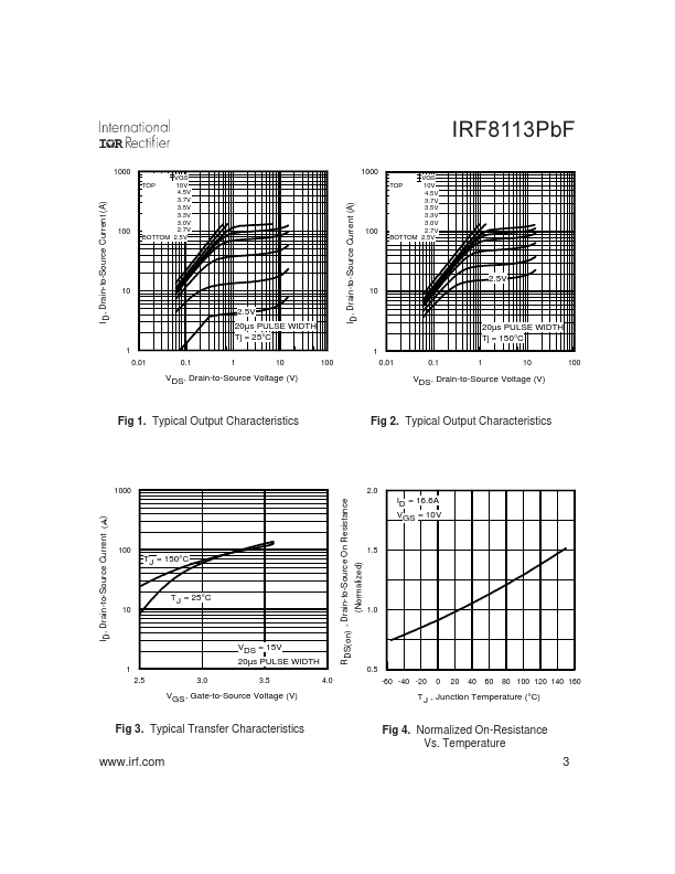
river between the time that the threshold voltage has been reached and the time the drain current rises to Idmax at which time the drain voltage begins to change. Minimizing Qgs2 is a critical factor in reducing switching losses in Q1.
Qoss is the charge that must be supplied to the output capacitance of the MOSFET during every switching cycle. Figure A shows how Qoss is formed by the parallel combination of the voltage dependant (nonlinear) capacitances Cds and Cdg when multiplied by the power.
The following content is an automatically extracted verbatim text
from the original manufacturer datasheet and is provided for reference purposes only.
View original datasheet text
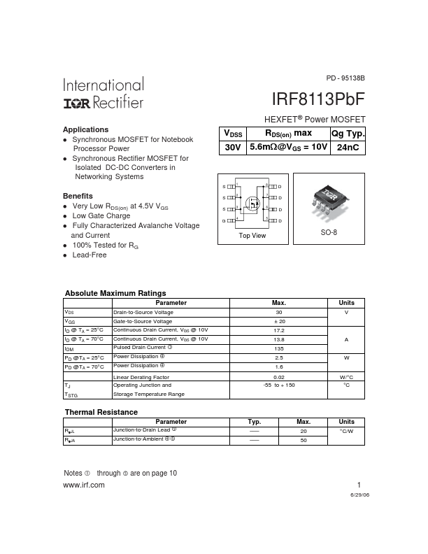
Applications l Synchronous MOSFET for Notebook
Processor Power l Synchronous Rectifier MOSFET for
Isolated DC-DC Converters in Networking Systems
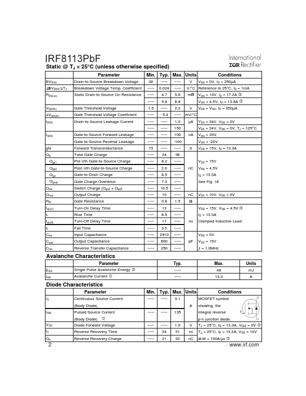
Benefits l Very Low RDS(on) at 4.5V VGS l Low Gate Charge l Fully Characterized Avalanche Voltage
and Current l 100% Tested for RG l Lead-Free
PD - 95138B
IRF8113PbF
HEXFET® Power MOSFET
VDSS
RDS(on) max Qg Typ.
:30V 5.
 IRF8113PbF Datasheet