Datasheet4U Logo Datasheet4U.com

ICS8602 - DIFFERENTIAL-TO-LVCMOS/LVTTL CLOCK GENERATOR

Datasheet Summary

Description

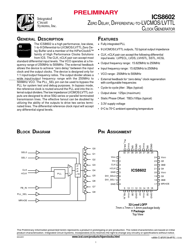
The ICS8602 is a high performance, low skew, ,&6 1-to-9 Differential-to-LVCMOS/LVTTL Zero DeHiPerClockS™ lay Buffer and a member of the HiPerClockS™ family of High Performance Clocks Solutions from ICS.

The CLK, nCLK pair can accept most standard differential input levels.

Features

  • Fully integrated PLL.
  • 9 LVCMOS/LVTTL outputs, 7Ω typical output impedance.
  • CLK, nCLK pair can accept the following differential input levels: LVPECL, LVDS, LVHSTL, SSTL, HCSL.
  • Output frequency range: 15.625MHz to 250MHz.
  • Input frequency range: 15.625MHz to 250MHz.
  • VCO range: 250MHz to 500MHz.
  • External feedback for “zero delay” clock regeneration with configurable frequencies.
  • Cycle-to-cycle jitter: 36ps (typical).

📥 Download Datasheet

Datasheet preview – ICS8602

Datasheet Details

Part number ICS8602
Manufacturer Integrated Circuit Systems
File Size 143.02 KB
Description DIFFERENTIAL-TO-LVCMOS/LVTTL CLOCK GENERATOR
Datasheet download datasheet ICS8602 Datasheet
Additional preview pages of the ICS8602 datasheet.
Other Datasheets by Integrated Circuit Systems

Full PDF Text Transcription

Click to expand full text
PRELIMINARY Integrated Circuit Systems, Inc. ICS8602 ZERO DELAY, DIFFERENTIAL-TO-LVCMOS/LVTTL CLOCK GENERATOR FEATURES • Fully integrated PLL • 9 LVCMOS/LVTTL outputs, 7Ω typical output impedance • CLK, nCLK pair can accept the following differential input levels: LVPECL, LVDS, LVHSTL, SSTL, HCSL • Output frequency range: 15.625MHz to 250MHz • Input frequency range: 15.625MHz to 250MHz • VCO range: 250MHz to 500MHz • External feedback for “zero delay” clock regeneration with configurable frequencies • Cycle-to-cycle jitter: 36ps (typical) • Output skew: 125ps (maximum) • Static Phase Offset: TBD±100ps (typical) • 3.
Published: |