The following content is an automatically extracted verbatim text
from the original manufacturer datasheet and is provided for reference purposes only.
View original datasheet text
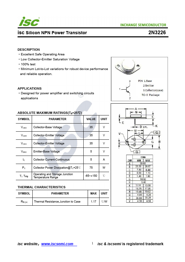
isc Silicon NPN Power Transistor
DESCRIPTION ·Excellent Safe Operating Area ·Low Collector-Emitter Saturation Voltage ·100% test ·Minimum Lot-to-Lot variations for robust device performance
and reliable operation.
APPLICATIONS ·Designed for power amplifier and switching circuits
applications
ABSOLUTE MAXIMUM RATINGS(Ta=25℃)
SYMBOL
PARAMETER
VALUE
UNIT
VCBO
Collector-Base Voltage
35
V
VCER
Collector-Emitter Voltage
35
V
VCEO
Collector-Emitter Voltage
35
V
VEBO
Emitter-Base Voltage
5
V
IC
Collector Current-Continuous
5
A
PC
Collector Power Dissipation@TC=25℃
75
W
TJ, Tstg
Operating and Storage Junction Temperature Range
-65~+150 ℃
THERMAL CHARACTERISTICS
SYMBOL
PARAMETER
Rth j-c Thermal Resistance,Junction to Case
MAX UNIT 1.
 2N3226 Datasheet