FDMS3668S
Overview
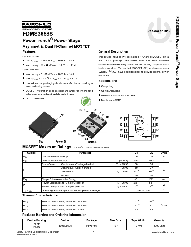
This device includes two specialized N-Channel MOSFETs in a dual PQFN package. The switch node has been internally connected to enable easy placement and routing of synchronous buck converters.
- Max rDS(on) = 8 mΩ at VGS = 10 V, ID = 13 A
- Max rDS(on) = 11 mΩ at VGS = 4.5 V, ID = 11 A Q2: N-Channel
- Max rDS(on) = 5 mΩ at VGS = 10 V, ID = 18 A
- Max rDS(on) = 5.2 mΩ at VGS = 4.5 V, ID = 17 A
- Low inductance packaging shortens rise/fall times, resulting in lower switching losses
- MOSFET integration enables optimum layout for lower circuit inductance and reduced switch node ringing
- RoHS Compliant December 2012