Click to expand full text
Revision History
Revision 0.1 (Jul. 2010) - First release.
Revision 0.2 (Sep. 2010) - Delete CL=2, page 2, 8, 17 - Add 166MHz@2.5-3-3; 200MHz@3-3-3, page 2
EM42AM1684RTC
Sep. 2010
www.eorex.com 1/21
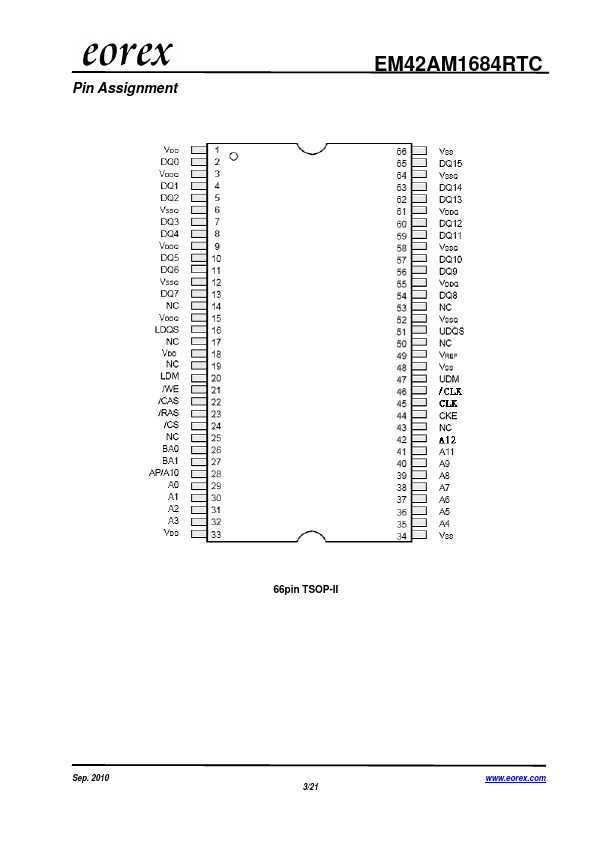
EM42AM1684RTC
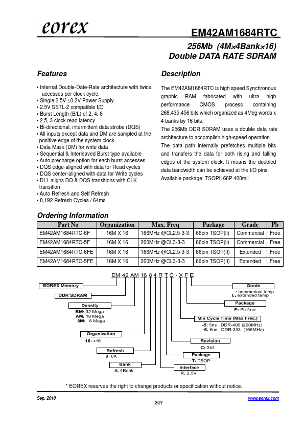
256Mb (4M×4Bank×16) Double DATA RATE SDRAM
Features
Description
• Internal Double-Date-Rate architecture with twice accesses per clock cycle.
• Single 2.5V ±0.2V Power Supply • 2.5V SSTL-2 compatible I/O • Burst Length (B/L) of 2, 4, 8 • 2.5, 3 clock read latency • Bi-directional, intermittent data strobe (DQS) • All inputs except data and DM are sampled at the positive edge of the system clock.
 EM42AM1684RTC Datasheet