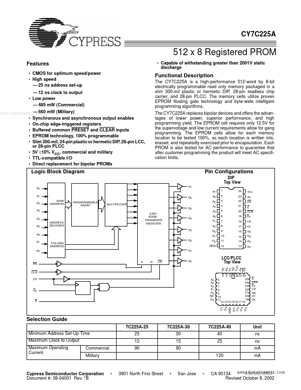
CY7C225A
Maximum Ratings[1]
DC Program Voltage (Pins 7, 18, 20) ........................... 13.0V
(Above which the useful life may be impaired. For user guide-
lines, not tested.)
Storage Temperature ..................................... −65°C to +150°C
Static Discharge Voltage............................................ >2001V
(per MIL-STD-883, Method 3015)
Latch-Up Current..................................................... >200 mA
Ambient Temperature with
Power Applied.................................................. −55°C to +125°C
Supply Voltage to Ground Potential
(Pin 24 to Pin 12).................................................−0.5V to +7.0V
Operating Range
Range
Ambient
Temperature
VCC
DC Voltage Applied to Outputs
in High Z State .....................................................−0.5V to +7.0V
DC Input Voltage .................................................−3.0V to +7.0V
www.DataSheet4U.com
Commercial
Military[2]
0°C to +70°C
−55°C to +125°C
5V ± 10%
5V ± 10%
Electrical Characteristics Over the Operating Range[3,4]
Parameter
Description
Test Conditions
Min.
Max.
Unit
VOH
Output HIGH Voltage
VCC = Min., IOH = −4.0 mA
VIN = VIH or VIL
2.4 V
VOL
Output LOW Voltage
VCC = Min., IOL = 16 mA
VIN = VIH or VIL
0.4 V
VIH Input HIGH Level
Guaranteed Input Logical HIGH Voltage for
All Inputs
2.0
V
VIL Input LOW Level
Guaranteed Input Logical LOW Voltage for All
Inputs
0.8 V
IIX
Input Leakage Current
GND < VIN < VCC
−10 +10 µA
VCD Input Clamp Diode Voltage Note 4
IOZ
Output Leakage Current
GND < VOUT < VCC, Output Disabled[5]
−10 +10 µA
IOS Output Short Circuit Current VCC = Max., VOUT = 0.0V[6]
−20 −90 mA
ICC
Power Supply Current
IOUT = 0 mA
VCC = Max.
Commercial
Military
90 mA
120
VPP
IPP
VIHP
Programming Supply Voltage
Programming Supply Current
Input HIGH Programming
Voltage
12 13 V
50 mA
3.0 V
VILP Input LOW Programming
Voltage
0.4 V
Capacitance[4]
Parameter
Description
Test Conditions
Max.
CIN
COUT
Input Capacitance
Output Capacitance
TA = 25°C, f = 1 MHz,
VCC =5.0V
10
10
Notes:
1. The Voltage on any input or I/O pin cannot exceed the power pin during power-up.
2. TA is the “instant on” case temperature.
3. See the last page of this specification for Group A subgroup testing information.
4. See the “Introduction to CMOS PROMs” section of the Cypress Data Book for general information on testing.
5. For devices using the synchronous enable, the device must be clocked after applying these voltages to perform this measurement.
6. For test purposes, not more than one output at a time should be shorted. Short circuit test duration should not exceed 30 seconds.
Unit
pF
pF
Document #: 38-04001 Rev. *B
Page 2 of 9