S-19630A Description
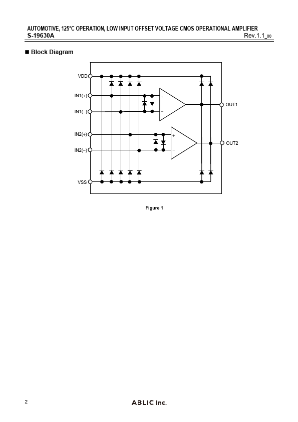
OUT1.
S-19630A Key Features
- Low input offset voltage
- Low input offset voltage drift
- Operation power supply voltage range
- Low current consumption (Per circuit)
- Low input noise voltage
- Low input noise voltage density
- Built-in output current limit circuit
- Internal phase pensation
- Rail-to-Rail input and output
- Operation temperature range