Click to expand full text
S-19610A
www.ablicinc.com © ABLIC Inc., 2014
MINI ANALOG SERIES FOR AUTOMOTIVE 125°C OPERATION CMOS OPERATIONAL AMPLIFIER
Rev.1.0_02
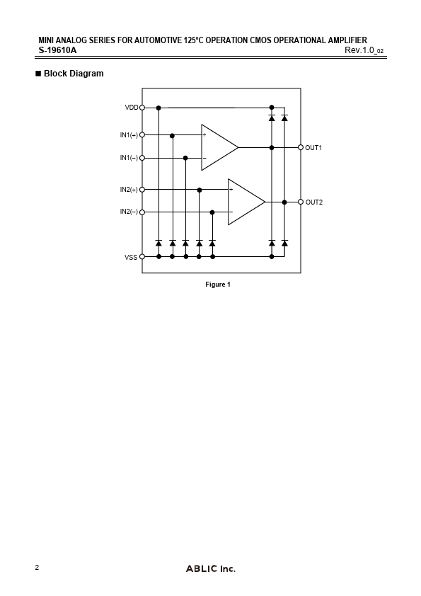
The mini-analog series is a group of ICs that incorporate a general purpose analog circuit in a small package. The S-19610A is a CMOS type operational amplifier that has a phase compensation circuit, and operates at a low voltage with low current consumption. The S-19610A is a dual operational amplifier (with 2 circuits).
Caution This product can be used in vehicle equipment and in-vehicle equipment. Before using the product in the purpose, contact to ABLIC Inc. is indispensable.
Features
Low input offset voltage:
VIO = 6.0 mV max. (Ta = 40C to 125C)
Operation power supply voltage range: VDD = 2.70 V to 5.
 S-19610A Datasheet