Datasheet4U Logo Datasheet4U.com

S-19611A - CMOS OPERATIONAL AMPLIFIER

Description

Output pin 1 Inverted input pin 1 Non-inverted input pin 1 GND pin Non-inverted input pin 2 Inverted input pin 2 Output pin 2 Positive power supply pin 4 AUTOMOTIVE, 105°C OPERATION, LOW INPUT OFFSET VOLTAGE CMOS OPERATIONAL AMPLIFIER Rev.1.2_00 S-19611A Absolute Maximum Ratings Table 4

Features

  • Low input offset voltage:.
  • Operation power supply voltage range:.
  • Low current consumption (Per circuit):.
  • Internal phase compensation:.
  • Rail-to-Rail input and output.
  • Operation temperature range:.
  • Lead-free (Sn 100%), halogen-free.
  • AEC-Q100 qualified.
  • 1 VIO = +17 μV max. (Ta = +25°C) VIO = +100 μV max. (Ta =.
  • 40°C to +105°C) VDD = 2.65 V to 5.50 V IDD = 200 μA typ. No external parts required Ta =.
  • 40°C t.

📥 Download Datasheet

Datasheet preview – S-19611A

Datasheet Details

Part number S-19611A
Manufacturer ABLIC
File Size 554.00 KB
Description CMOS OPERATIONAL AMPLIFIER
Datasheet download datasheet S-19611A Datasheet
Additional preview pages of the S-19611A datasheet.
Other Datasheets by ABLIC

Full PDF Text Transcription

Click to expand full text
S-19611A www.ablic.com © ABLIC Inc., 2014-2020 AUTOMOTIVE, 105°C OPERATION, LOW INPUT OFFSET VOLTAGE CMOS OPERATIONAL AMPLIFIER Rev.1.2_00 
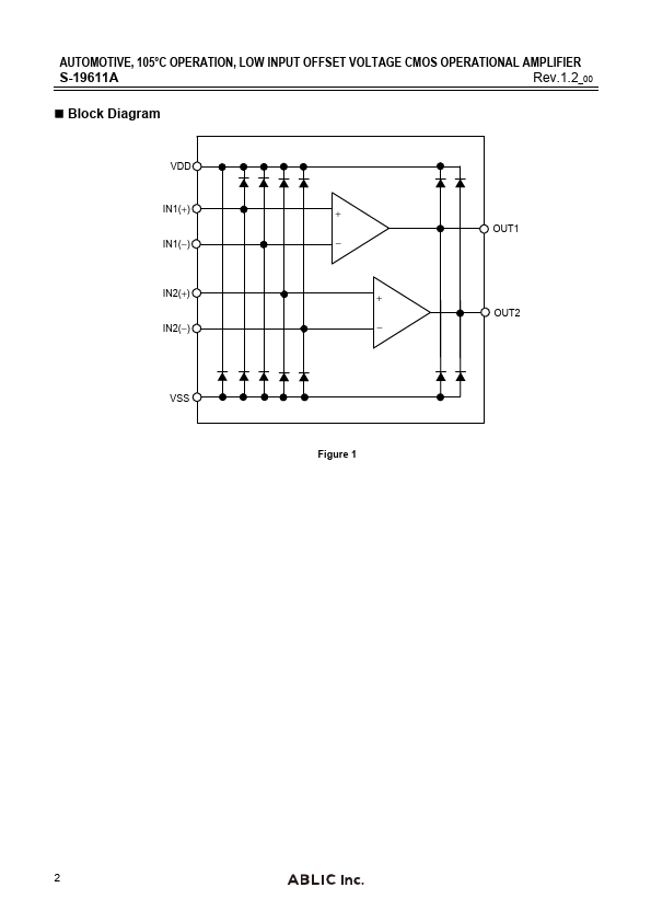
This IC incorporates a general purpose analog circuit in a small package. This is a zero-drift operational amplifier with Rail-to-Rail input and output, which uses auto-zeroing techniques to provide low input offset voltage. This IC is suitable for applications requiring less offset voltage. The S-19611AB is a dual operational amplifier (2 circuits). Caution This product can be used in vehicle equipment and in-vehicle equipment. Before using the product for these purposes, it is imperative to contact our sales representatives.
Published: |