Datasheet Details
| Part number | 74HCT175-Q100 |
|---|---|
| Manufacturer | Nexperia |
| File Size | 256.41 KB |
| Description | Quad D-type flip-flop |
| Datasheet |
 74HCT175-Q100 Datasheet 74HCT175-Q100 Datasheet
|
|
|
Download the 74HCT175-Q100 datasheet PDF. This datasheet also covers the 74HC175-Q100 variant, as both devices belong to the same quad d-type flip-flop family and are provided as variant models within a single manufacturer datasheet.
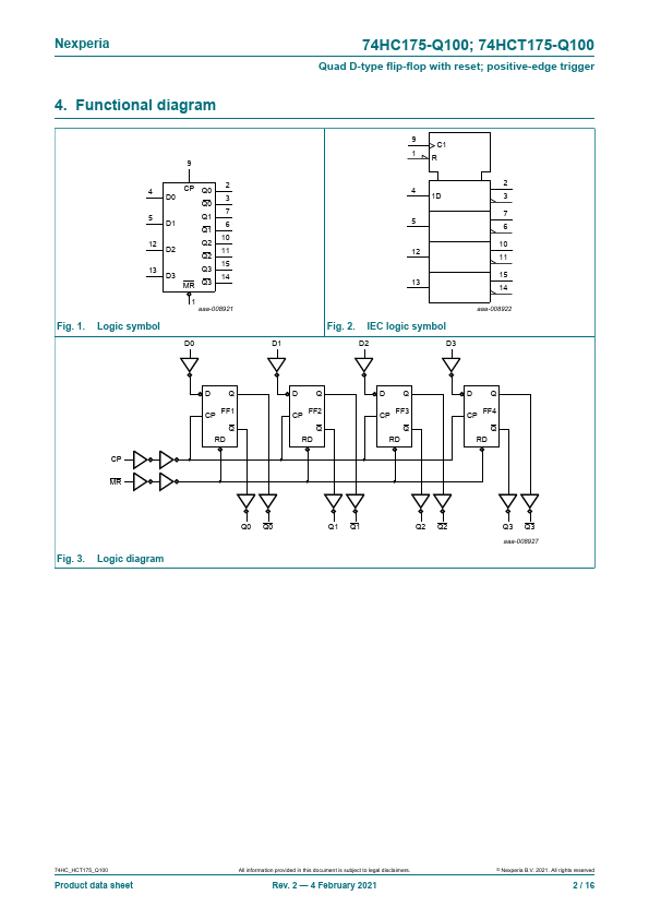
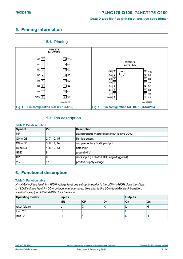
The 74HC175-Q100; 74HCT175-Q100 are quad positive edge-triggered D-type flip-flops with individual data inputs (Dn) and both Qn and Qn outputs.
The common clock (CP) and master reset (MR) inputs load and reset all flip-flops simultaneously.
| Part number | 74HCT175-Q100 |
|---|---|
| Manufacturer | Nexperia |
| File Size | 256.41 KB |
| Description | Quad D-type flip-flop |
| Datasheet |
74HCT175-Q100 Datasheet
|
|
|
|
Note: Below is a high-fidelity text extraction (approx. 800 characters) for 74HCT175-Q100. For precise diagrams, and layout, please refer to the original PDF.
74HC175-Q100; 74HCT175-Q100 Quad D-type flip-flop with reset; positive-edge trigger Rev. 2 — 4 February 2021 Product data sheet 1. General description The 74HC175-Q100; 7...
| Part Number | Description |
|---|---|
| 74HCT175 | Quad D-type flip-flop |
| 74HCT175D | Quad D-type flip-flop |
| 74HCT173 | Quad D-type flip-flop |
| 74HCT173D | Quad D-type flip-flop |
| 74HCT174 | Hex D-type flip-flop |
| 74HCT174-Q100 | Hex D-type flip-flop |
| 74HCT174D | Hex D-type flip-flop |
| 74HCT10 | Triple 3-input NAND gate |
| 74HCT10-Q100 | Triple 3-input NAND gate |
| 74HCT107 | Dual JK flip-flop |