Datasheet Details
| Part number | 74ALVCH16952DGG |
|---|---|
| Manufacturer | nexperia |
| File Size | 185.39 KB |
| Description | 16-bit registered transceiver |
| Datasheet |
 74ALVCH16952DGG Datasheet 74ALVCH16952DGG Datasheet
|
|
|
Download the 74ALVCH16952DGG datasheet PDF. This datasheet also covers the 74ALVCH16952 variant, as both devices belong to the same 16-bit registered transceiver family and are provided as variant models within a single manufacturer datasheet.
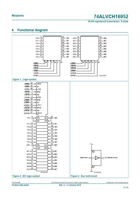
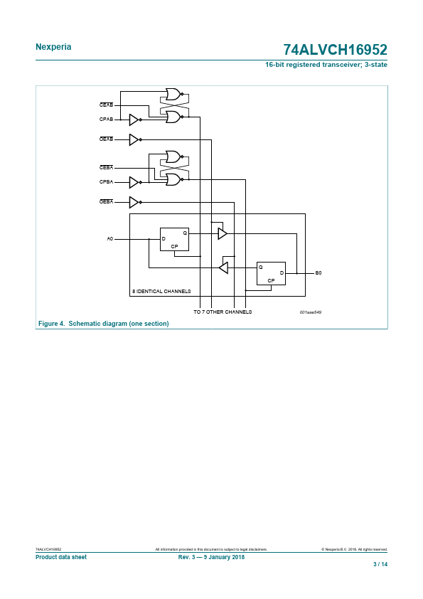
The 74ALVCH16952 consists of two sections, each containing a dual octal non-inverting registered transceiver.
Two 8-bit back to back registers store data flowing in both directions between two bidirectional buses.
| Part number | 74ALVCH16952DGG |
|---|---|
| Manufacturer | nexperia |
| File Size | 185.39 KB |
| Description | 16-bit registered transceiver |
| Datasheet |
74ALVCH16952DGG Datasheet
|
|
|
|
| Part Number | Description | Manufacturer |
|---|---|---|
| 74ALVCH16952 | 16-bit registered transceiver | NXP |
| 74ALVCH162240 | Low Voltage 16-Bit Inverting Buffer/Line Driver | Fairchild Semiconductor |
| 74ALVCH162244 | 16-bit buffer/line driver | NXP |
| 74ALVCH162244 | Low Voltage 16-Bit Buffer/Line Driver | Fairchild Semiconductor |
| 74ALVCH162244 | 3.3V CMOS 16-BIT BUFFER/DRIVER | Renesas |
| Part Number | Description |
|---|---|
| 74ALVCH16952 | 16-bit registered transceiver |
| 74ALVCH162244 | 16-bit buffer/line driver |
| 74ALVCH162244DGG | 16-bit buffer/line driver |
| 74ALVCH162245 | 16-bit bus transceiver |
| 74ALVCH16244 | 16-bit buffer/line driver |