Click to expand full text
Product Folder
Sample & Buy
Technical Documents
Tools & Software
Support & Community
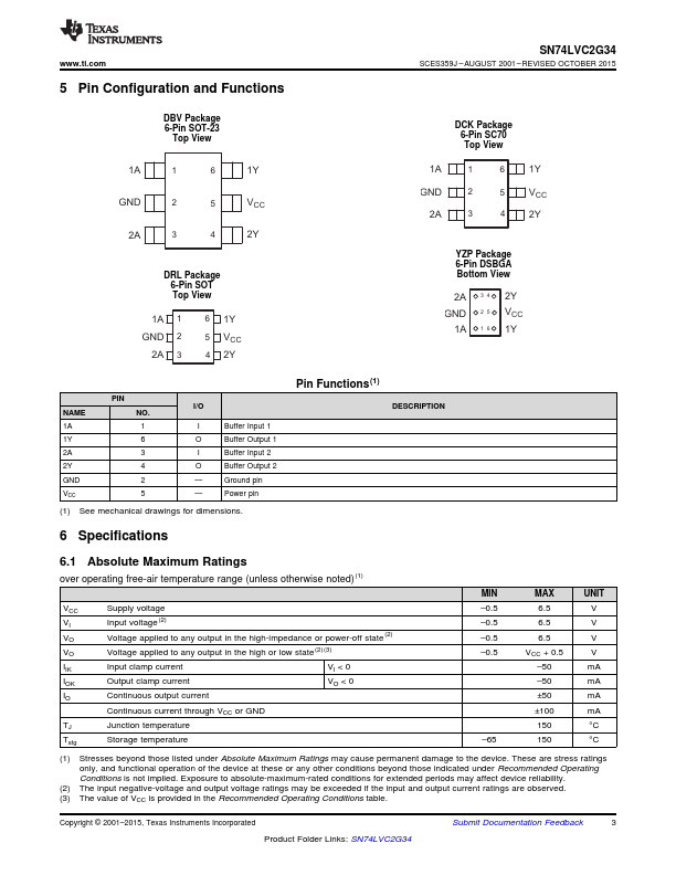
SN74LVC2G34
SCES359J – AUGUST 2001 – REVISED OCTOBER 2015
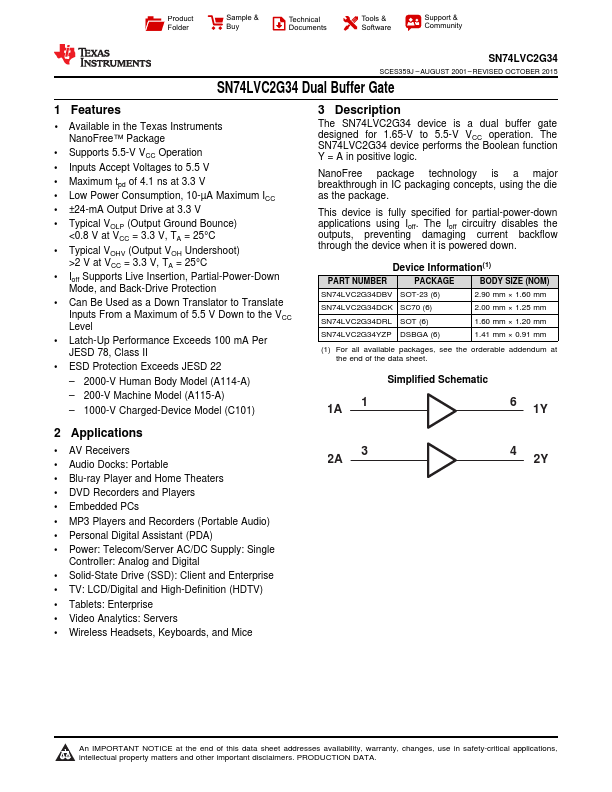
SN74LVC2G34 Dual Buffer Gate
1 Features
•1 Available in the Texas Instruments NanoFree™ Package
• Supports 5.5-V VCC Operation • Inputs Accept Voltages to 5.5 V
• Maximum tpd of 4.1 ns at 3.3 V • Low Power Consumption, 10-µA Maximum ICC • ±24-mA Output Drive at 3.3 V
• Typical VOLP (Output Ground Bounce) <0.8 V at VCC = 3.3 V, TA = 25°C
• Typical VOHV (Output VOH Undershoot) >2 V at VCC = 3.3 V, TA = 25°C
• Ioff Supports Live Insertion, Partial-Power-Down Mode, and Back-Drive Protection
• Can Be Used as a Down Translator to Translate Inputs From a Maximum of 5.
 SN74LVC2G34 Datasheet