Datasheet Details
| Part number | SN74LVC1G125 |
|---|---|
| Manufacturer | Texas Instruments |
| File Size | 2.48 MB |
| Description | Single Bus Buffer Gate |
| Datasheet |
 SN74LVC1G125 Datasheet SN74LVC1G125 Datasheet
|
|
|
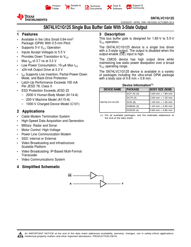
This bus buffer gate is designed for 1.65-V to 5.5-V VCC operation.
The SN74LVC1G125 device is a single line driver with a 3-state output.
The output is disabled when the output-enable (OE) input is high.
| Part number | SN74LVC1G125 |
|---|---|
| Manufacturer | Texas Instruments |
| File Size | 2.48 MB |
| Description | Single Bus Buffer Gate |
| Datasheet |
SN74LVC1G125 Datasheet
|
|
|
|
| Part Number | Description | Manufacturer |
|---|---|---|
| SN74LVC1G125 | high performance non-inverting buffer | UMW |
| SN74LVC1G34 | Single buffer | UMW |
| SN74L71 | AND-Gate R-S Master-Slave F-F | National Semiconductor |
| SN74L74N | Dual D-Type Flip-Flop | ETC |
| SN74LS00 | QUAD 2-INPUT NAND GATE | Motorola |
| Part Number | Description |
|---|---|
| SN74LVC1G125-EP | Single Bus Buffer Gate |
| SN74LVC1G125-Q1 | Single Bus Buffer Gate |
| SN74LVC1G123 | Single Retriggerable Monostable Multivibrator |
| SN74LVC1G126 | Single Bus Buffer Gate |
| SN74LVC1G126-EP | Single Bus Buffer Gate |
The following content is an automatically extracted verbatim text from the original manufacturer datasheet and is provided for reference purposes only.