Datasheet Details
| Part number | SN74LVC126A |
|---|---|
| Manufacturer | Texas Instruments |
| File Size | 705.93 KB |
| Description | Quadruple Bus Buffer |
| Datasheet |
 SN74LVC126A Datasheet SN74LVC126A Datasheet
|
|
|
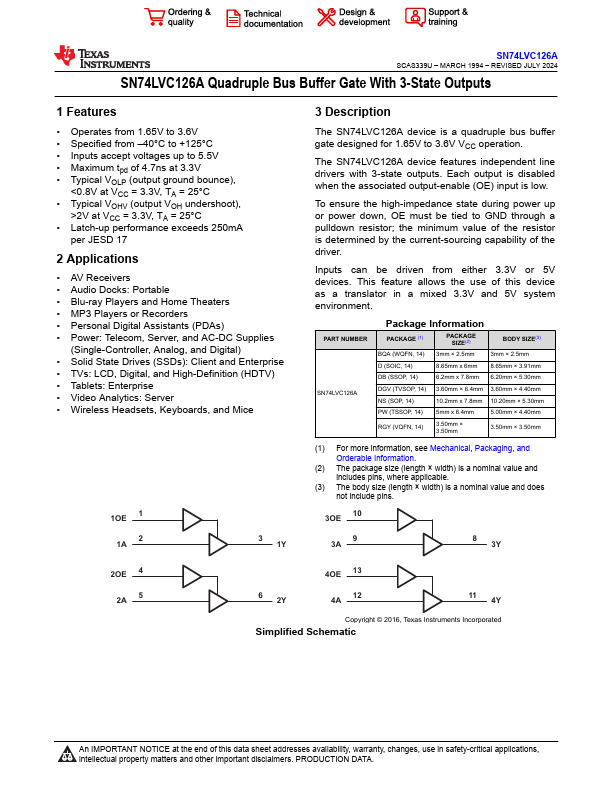
The SN74LVC126A device is a quadruple bus buffer gate designed for 1.65V to 3.6V VCC operation.
| Part number | SN74LVC126A |
|---|---|
| Manufacturer | Texas Instruments |
| File Size | 705.93 KB |
| Description | Quadruple Bus Buffer |
| Datasheet |
SN74LVC126A Datasheet
|
|
|
|
| Part Number | Description | Manufacturer |
|---|---|---|
| SN74LVC1G125 | high performance non-inverting buffer | UMW |
| SN74LVC1G34 | Single buffer | UMW |
| SN74L71 | AND-Gate R-S Master-Slave F-F | National Semiconductor |
| SN74L74N | Dual D-Type Flip-Flop | ETC |
| SN74LS00 | QUAD 2-INPUT NAND GATE | Motorola |
| Part Number | Description |
|---|---|
| SN74LVC126A-Q1 | Automotive Quadruple Bus Buffer Gate |
| SN74LVC125A | Quadruple Bus Buffer Gate |
| SN74LVC125A-EP | Quadruple Bus Buffer Gate |
| SN74LVC125A-Q1 | Automotive Quadruple Bus Buffer Gate |
| SN74LVC10A | TRIPLE 3-INPUT POSITIVE-NAND GATE |