Click to expand full text
Product Folder
Order Now
Technical Documents
Tools & Software
Support & Community
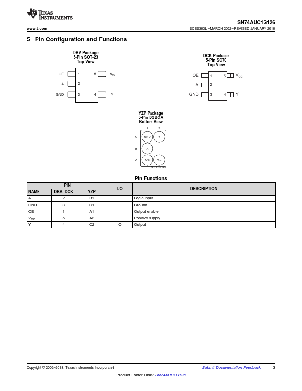
SN74AUC1G126
SCES383L – MARCH 2002 – REVISED JANUARY 2018
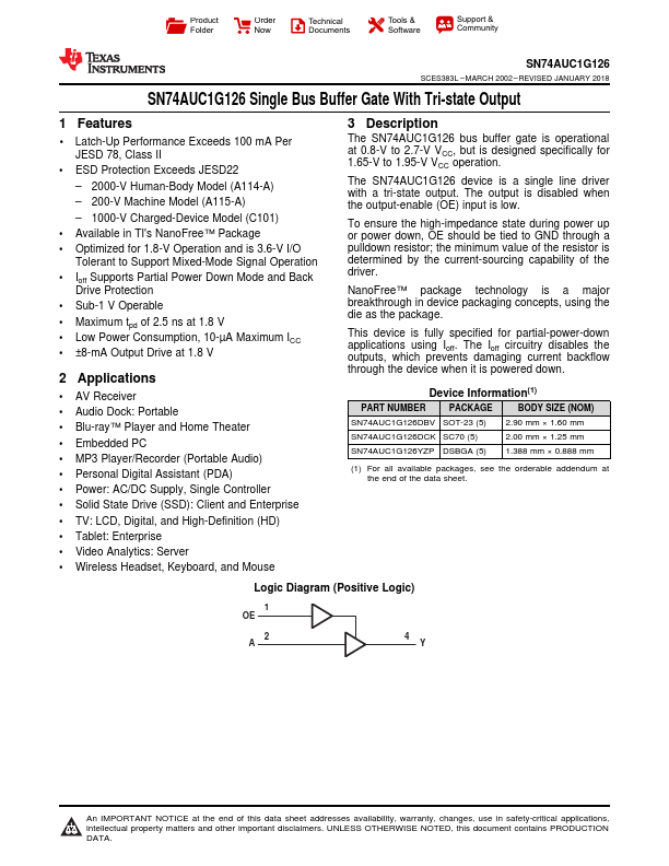
SN74AUC1G126 Single Bus Buffer Gate With Tri-state Output
1 Features
•1 Latch-Up Performance Exceeds 100 mA Per JESD 78, Class II
• ESD Protection Exceeds JESD22 – 2000-V Human-Body Model (A114-A) – 200-V Machine Model (A115-A) – 1000-V Charged-Device Model (C101)
• Available in TI's NanoFree™ Package • Optimized for 1.8-V Operation and is 3.6-V I/O
Tolerant to Support Mixed-Mode Signal Operation • Ioff Supports Partial Power Down Mode and Back
Drive Protection • Sub-1 V Operable • Maximum tpd of 2.5 ns at 1.8 V • Low Power Consumption, 10-µA Maximum ICC • ±8-mA Output Drive at 1.
 SN74AUC1G126 Datasheet