Datasheet Details
| Part number | SN65MLVD207 |
|---|---|
| Manufacturer | Texas Instruments |
| File Size | 888.11 KB |
| Description | MULTIPOINT-LVDS LINE DRIVER AND RECEIVER |
| Datasheet |
 SN65MLVD207 Datasheet SN65MLVD207 Datasheet
|
|
|
Download the SN65MLVD207 datasheet PDF. This datasheet also covers the SN65MLVD201 variant, as both devices belong to the same multipoint-lvds line driver and receiver family and are provided as variant models within a single manufacturer datasheet.
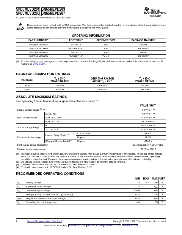
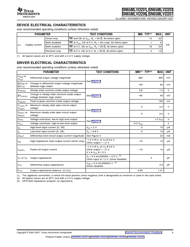
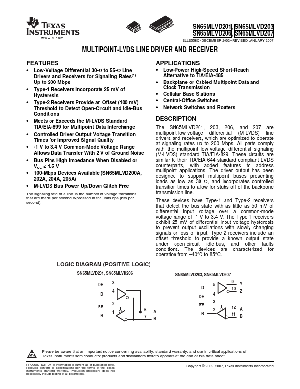
The SN65MLVD201, 203, 206, and 207 are multipoint-low-voltage differential (M-LVDS) line drivers and receivers, which are optimized to operate at signaling rates up to 200 Mbps.
All parts comply with the multipoint low-voltage differential signaling (M-LVDS) standard TIA/EIA-899.
| Part number | SN65MLVD207 |
|---|---|
| Manufacturer | Texas Instruments |
| File Size | 888.11 KB |
| Description | MULTIPOINT-LVDS LINE DRIVER AND RECEIVER |
| Datasheet |
SN65MLVD207 Datasheet
|
|
|
|
| Part Number | Description |
|---|---|
| SN65MLVD200 | MULTIPOINT-LVDS LINE DRIVERS AND RECEIVERS |
| SN65MLVD200A | Multipoint-LVDS Line Driver and Receiver |
| SN65MLVD200B | Multipoint-LVDS Line Drivers and Receivers |
| SN65MLVD201 | MULTIPOINT-LVDS LINE DRIVER AND RECEIVER |
| SN65MLVD202 | MULTIPOINT-LVDS LINE DRIVERS AND RECEIVERS |
| SN65MLVD202A | Multipoint-LVDS Line Driver and Receiver |
| SN65MLVD202B | Multipoint-LVDS Line Drivers and Receivers |
| SN65MLVD203 | MULTIPOINT-LVDS LINE DRIVER AND RECEIVER |
| SN65MLVD204 | MULTIPOINT-LVDS LINE DRIVERS AND RECEIVERS |
| SN65MLVD204A | Multipoint-LVDS Line Driver and Receiver |
The following content is an automatically extracted verbatim text from the original manufacturer datasheet and is provided for reference purposes only.