Datasheet Details
| Part number | SN65LVDS16 |
|---|---|
| Manufacturer | Texas Instruments |
| File Size | 883.38 KB |
| Description | 2.5-V/3.3-V OSCILLATOR GAIN STAGE/BUFFERS |
| Datasheet |
 SN65LVDS16 Datasheet SN65LVDS16 Datasheet
|
|
|
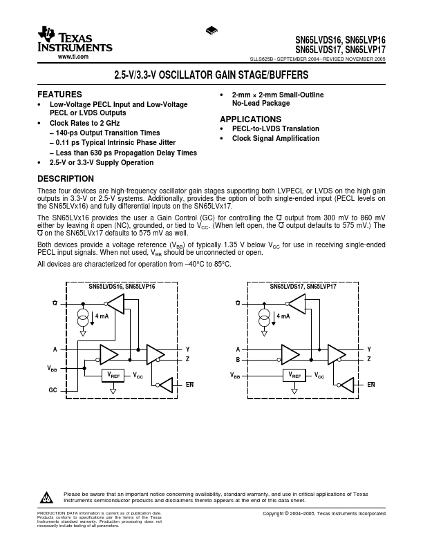
These four devices are high-frequency oscillator gain stages supporting both LVPECL or LVDS on the high gain outputs in 3.3-V or 2.5-V systems.
Additionally, provides the option of both single-ended input (PECL levels on the SN65LVx16) and fully differential inputs on the SN65LVx17.
| Part number | SN65LVDS16 |
|---|---|
| Manufacturer | Texas Instruments |
| File Size | 883.38 KB |
| Description | 2.5-V/3.3-V OSCILLATOR GAIN STAGE/BUFFERS |
| Datasheet |
SN65LVDS16 Datasheet
|
|
|
|
| Part Number | Description | Manufacturer |
|---|---|---|
| SN65004 | One Channel Direct Drive Speech Controller | SONiX Technology Company |
| SN65007 | One Channel Direct Drive Speech Controller | SONiX Technology Company |
| SN65010 | One Channel Direct Drive Speech Controller | SONiX Technology Company |
| SN65012 | One Channel Direct Drive Speech Controller | SONiX Technology Company |
| SN65016 | One Channel Direct Drive Speech Controller | SONiX Technology Company |
| Part Number | Description |
|---|---|
| SN65LVDS1 | High-Speed Differential Line Drivers/Receivers |
| SN65LVDS100 | Differential Translator/Repeater |
| SN65LVDS101 | Differential Translator/Repeater |
| SN65LVDS104 | 4-Port LVDS and 4-Port TTL-to-LVDS Repeaters |
| SN65LVDS105 | 4-Port LVDS and 4-Port TTL-to-LVDS Repeaters |