Datasheet Details
| Part number | SCAN92LV090 |
|---|---|
| Manufacturer | Texas Instruments |
| File Size | 881.72 KB |
| Description | 9-Channel Bus LVDS Transceiver |
| Datasheet |
 SCAN92LV090 Datasheet SCAN92LV090 Datasheet
|
|
|
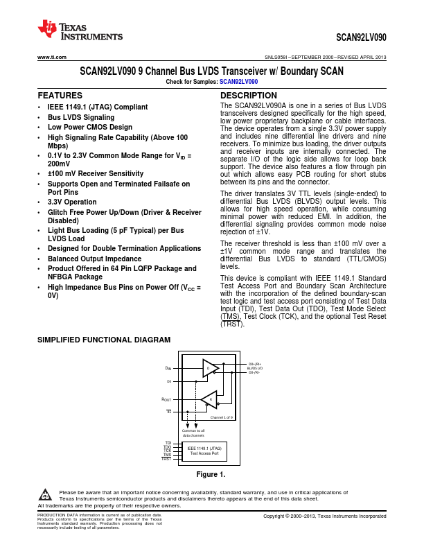
The SCAN92LV090A is one in a series of Bus LVDS transceivers designed specifically for the high speed, low power proprietary backplane or cable interfaces.
The device operates from a single 3.3V power supply and includes nine differential line drivers and nine receivers.
| Part number | SCAN92LV090 |
|---|---|
| Manufacturer | Texas Instruments |
| File Size | 881.72 KB |
| Description | 9-Channel Bus LVDS Transceiver |
| Datasheet |
SCAN92LV090 Datasheet
|
|
|
|
| Part Number | Description | Manufacturer |
|---|---|---|
| SCAN92LV090 | 9 Channel Bus LVDS Transceiver | National Semiconductor |
| SCAN921023 | 20-66 MHz 10 Bit Bus LVDS Serializer and Deserializer | National Semiconductor |
| SCAN921025 | 30-80 MHz 10-Bit Bus LVDS Serializer and Deserializer | National Semiconductor |
| SCAN921025H | High Temperature 20-80 MHz 10 Bit Bus LVDS SerDes | National Semiconductor |
| SCAN921224 | 20-66 MHz 10 Bit Bus LVDS Serializer and Deserializer | National Semiconductor |
| Part Number | Description |
|---|---|
| SCAN921023 | 20-66 MHz 10-Bit Bus LVDS Serializer and Deserializer |
| SCAN921025 | 30-80 MHz 10-Bit Bus LVDS Serializer and Deserializer |
| SCAN921025H | High Temperature 20-80 MHz 10-Bit Bus LVDS SerDes |
| SCAN921224 | 20-66 MHz 10-Bit Bus LVDS Serializer and Deserializer |
| SCAN921226 | 30-80 MHz 10-Bit Bus LVDS Serializer and Deserializer |
The following content is an automatically extracted verbatim text from the original manufacturer datasheet and is provided for reference purposes only.