Click to expand full text
Product Folder
Order Now
Technical Documents
Tools & Software
Support & Community
Reference Design
CSD18512Q5B
SLPS624A – DECEMBER 2016 – REVISED MARCH 2019
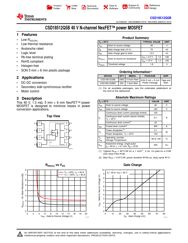
CSD18512Q5B 40 V N-channel NexFET™ power MOSFET
1 Features
•1 Low RDS(ON) • Low thermal resistance • Avalanche rated • Logic level • Pb-free terminal plating • RoHS compliant • Halogen-free • SON 5 mm × 6 mm plastic package
2 Applications
• DC-DC conversion • Secondary side synchronous rectifier • Motor control
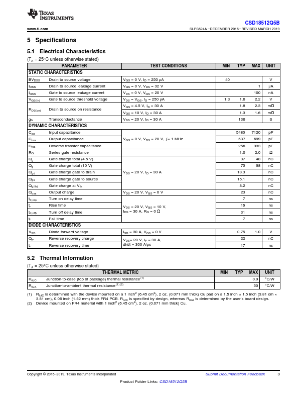
Product Summary
TA = 25°C VDS Drain to source voltage Qg Gate charge total (10 V) Qgd Gate charge gate to drain
RDS(on) Drain to source on resistance
VGS(th) Threshold voltage
TYPICAL VALUE
40
75
13.3
VGS = 4.5 V VGS = 10 V
1.6
1.8 1.
 CSD18512Q5B Datasheet