Click to expand full text
Product Folder
Sample & Buy
Technical Documents
Tools & Software
Support & Community
CSD18511Q5A
SLPS631 – DECEMBER 2016
CSD18511Q5A 40 V N-Channel NexFET™ Power MOSFET
1 Features
•1 Low RDS(ON) • Low Thermal Resistance • Avalanche Rated • Logic Level • Pb Free Terminal Plating • RoHS Compliant • Halogen Free • SON 5-mm × 6-mm Plastic Package
2 Applications
• DC-DC Conversion • Secondary Side Synchronous Rectifier • Battery Motor Control
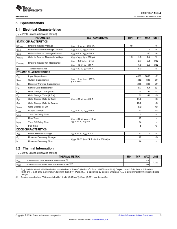
Product Summary
TA = 25°C VDS Drain-to-Source Voltage Qg Gate Charge Total (10 V) Qgd Gate Charge Gate-to-Drain
RDS(on) Drain-to-Source On-Resistance
VGS(th) Threshold Voltage
TYPICAL VALUE
40
63
11.2
VGS = 4.5 V VGS = 10 V
1.8
2.7 1.
 CSD18511Q5A Datasheet