Datasheet4U Logo Datasheet4U.com

CDCM1802 - Clock Buffer

Datasheet Summary

Description

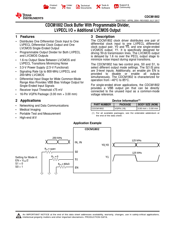
The CDCM1802 clock driver distributes one pair of differential clock input to one LVPECL differential clock output pair, Y0 and Y0, and one single-ended LVCMOS output, Y1.

It is specifically designed for driving 50-Ω transmission lines.

Features

  • 1 Distributes One Differential Clock Input to One LVPECL Differential Clock Output and One LVCMOS Single-Ended Output.
  • Programmable Output Divider for Both LVPECL and LVCMOS Outputs.
  • 1.6-ns Output Skew Between LVCMOS and LVPECL Transitions Minimizing Noise.
  • 3.3-V Power Supply (2.5-V Functional).
  • Signaling Rate Up to 800-MHz LVPECL and 200-MHz LVCMOS.
  • Differential Input Stage for Wide Common-Mode Range Also Provides VBB Bias Voltage Output for.

📥 Download Datasheet

Datasheet preview – CDCM1802

Datasheet Details

Part number CDCM1802
Manufacturer Texas Instruments
File Size 1.65 MB
Description Clock Buffer
Datasheet download datasheet CDCM1802 Datasheet
Additional preview pages of the CDCM1802 datasheet.
Other Datasheets by Texas Instruments

Full PDF Text Transcription

Click to expand full text
Product Folder Order Now Technical Documents Tools & Software Support & Community CDCM1802 SCAS759C – APRIL 2004 – REVISED JULY 2017 CDCM1802 Clock Buffer With Programmable Divider, LVPECL I/O + Additional LVCMOS Output 1 Features •1 Distributes One Differential Clock Input to One LVPECL Differential Clock Output and One LVCMOS Single-Ended Output • Programmable Output Divider for Both LVPECL and LVCMOS Outputs • 1.6-ns Output Skew Between LVCMOS and LVPECL Transitions Minimizing Noise • 3.3-V Power Supply (2.5-V Functional) • Signaling Rate Up to 800-MHz LVPECL and 200-MHz LVCMOS • Differential Input Stage for Wide Common-Mode Range Also Provides VBB Bias Voltage Output for Single-Ended Input Signals • Receiver Input Threshold ±75 mV • 16-Pin VQFN Package (3.00 mm × 3.
Published: |