Datasheet Details
| Part number | CD74HCT4075E |
|---|---|
| Manufacturer | Texas Instruments |
| File Size | 947.58 KB |
| Description | Triple 3-Input OR Gate |
| Datasheet |
 CD74HCT4075E Datasheet CD74HCT4075E Datasheet
|
|
|
Download the CD74HCT4075E datasheet PDF. This datasheet also covers the CD74HC4075 variant, as both devices belong to the same triple 3-input or gate family and are provided as variant models within a single manufacturer datasheet.
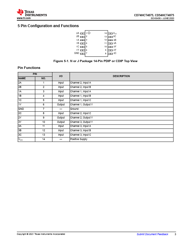
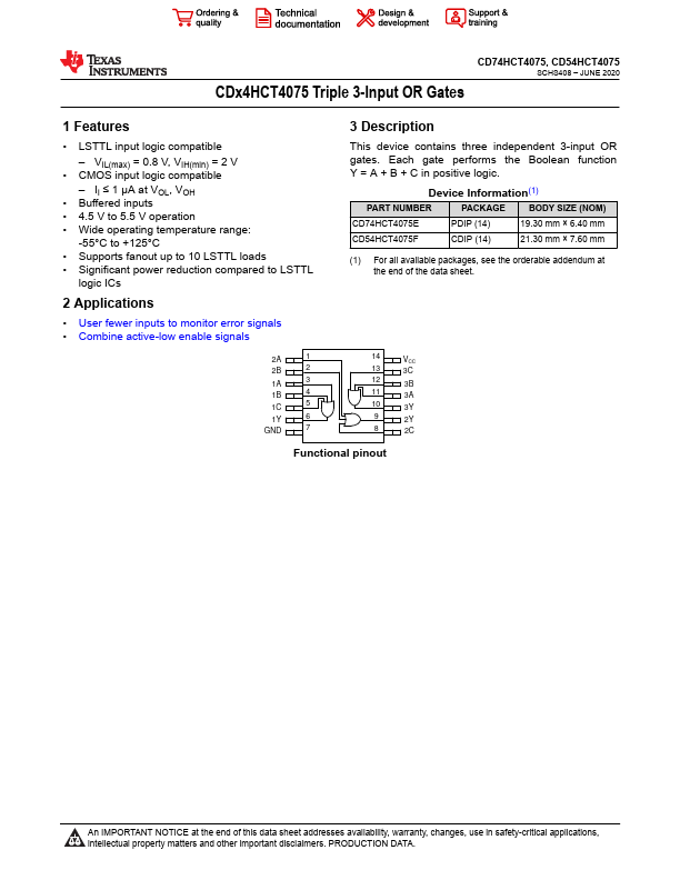
This device contains three independent 3-input OR gates.
Each gate performs the Boolean function Y = A + B + C in positive logic.
| Part number | CD74HCT4075E |
|---|---|
| Manufacturer | Texas Instruments |
| File Size | 947.58 KB |
| Description | Triple 3-Input OR Gate |
| Datasheet |
CD74HCT4075E Datasheet
|
|
|
|
Note: Below is a high-fidelity text extraction (approx. 800 characters) for CD74HCT4075E. For precise diagrams, and layout, please refer to the original PDF.
CD74HCT4075, CD54HCT4075 SCHS408 – JUNE 2020 CDx4HCT4075 Triple 3-Input OR Gates 1 Features • LSTTL input logic compatible – VIL(max) = 0.8 V, VIH(min) = 2 V • CMOS input...
| Part Number | Description |
|---|---|
| CD74HCT4075 | Triple 3-Input OR Gate |
| CD74HCT40103 | 8-Stage Synchronous Down Counters |
| CD74HCT40105 | 4-Bit x 16-Word FIFO Register |
| CD74HCT4020 | 14-Stage Binary Counter |
| CD74HCT4024 | 7-Stage Binary Ripple Counter |
| CD74HCT4040 | 12-Stage Binary Counter |
| CD74HCT4040E | 12-Stage Binary Counter |
| CD74HCT4040M | 12-Stage Binary Counter |
| CD74HCT4046A | Phase-Locked Loop |
| CD74HCT4051 | High-Speed CMOS Logic Analog Multiplexers/Demultiplexers |