Datasheet Details
| Part number | CD74HCT299 |
|---|---|
| Manufacturer | Texas Instruments |
| File Size | 894.45 KB |
| Description | 8-Bit Universal Shift Register |
| Datasheet |
 CD74HCT299 Datasheet CD74HCT299 Datasheet
|
|
|
Download the CD74HCT299 datasheet PDF. This datasheet also covers the CD74HC299 variant, as both devices belong to the same 8-bit universal shift register family and are provided as variant models within a single manufacturer datasheet.
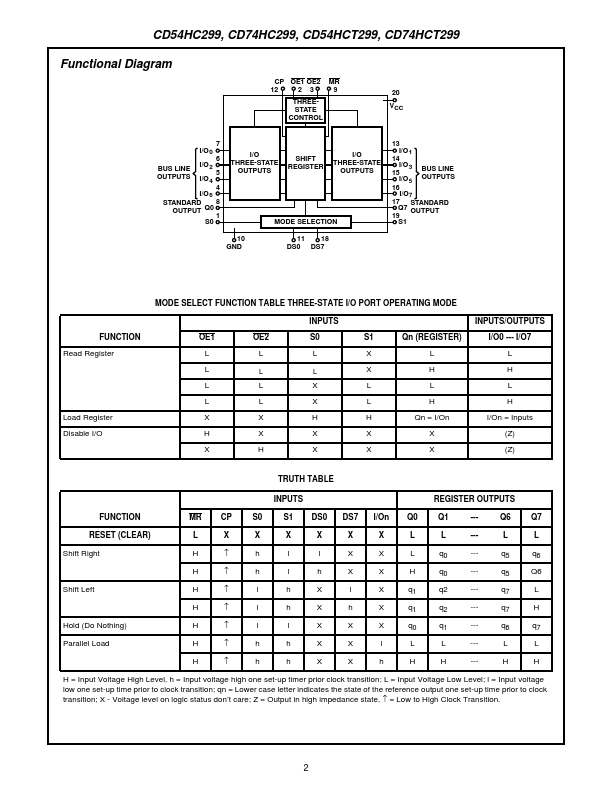
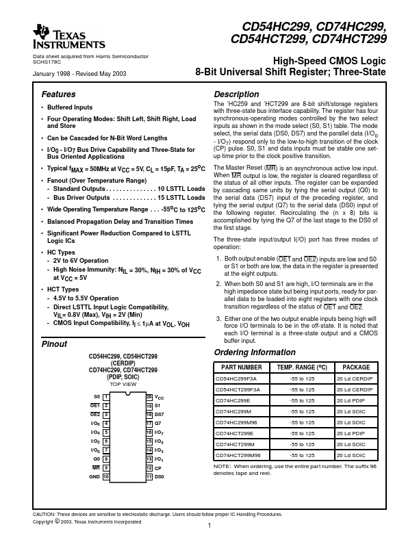
The ’HC259 and ’HCT299 are 8-bit shift/storage registers with three-state bus interface capability.
The register has four synchronous-operating modes controlled by the two select inputs as shown in the mode select (S0, S1) table.
| Part number | CD74HCT299 |
|---|---|
| Manufacturer | Texas Instruments |
| File Size | 894.45 KB |
| Description | 8-Bit Universal Shift Register |
| Datasheet |
CD74HCT299 Datasheet
|
|
|
|
Note: Below is a high-fidelity text extraction (approx. 800 characters) for CD74HCT299. For precise diagrams, and layout, please refer to the original PDF.
Data sheet acquired from Harris Semiconductor SCHS178C January 1998 - Revised May 2003 CD54HC299, CD74HC299, CD54HCT299, CD74HCT299 High-Speed CMOS Logic 8-Bit Universal ...
| Part Number | Description |
|---|---|
| CD74HCT297 | Digital Phase-Locked Loop |
| CD74HCT20 | Dual 4-Input NAND Gates |
| CD74HCT20E | Dual 4-Input NAND Gates |
| CD74HCT20M | Dual 4-Input NAND Gates |
| CD74HCT21 | High-Speed CMOS Logic Dual 4-Input AND Gate |
| CD74HCT221 | Dual Monostable Multivibrator |
| CD74HCT237 | High-Speed CMOS Logic 3 to 8-Line Decoder/Demultiplexer |
| CD74HCT238 | High-Speed CMOS Logic 3 to 8-Line Decoder/Demultiplexer Inverting/Noninverting |
| CD74HCT238E | High-Speed CMOS Logic 3 to 8-Line Decoder/Demultiplexer Inverting/Noninverting |
| CD74HCT238M | High-Speed CMOS Logic 3 to 8-Line Decoder/Demultiplexer Inverting/Noninverting |